Hardware Design Guide_V1.1
Document classification: □ Top secret □ Secret □ Internal information ■ Open
Copyright
The copyright of this manual belongs to Baoding Folinx Embedded Technology Co., Ltd. Without the written permission of our company, no organizations or individuals have the right to copy, distribute, or reproduce any part of this manual in any form, and violators will be held legally responsible.
Forlinx adheres to copyrights of all graphics and texts used in all publications in original or license-free forms.
The drivers and utilities used for the components are subject to the copyrights of the respective manufacturers. The license conditions of the respective manufacturer are to be adhered to. Related license expenses for the operating system and applications should be calculated/declared separately by the related party or its representatives.
Overview
This document applies to the FET-MX93xx-C and FET-MX91xx-C V1.3 System-on-Modules (SoMs). It describes the schematic design and PCB design of the peripheral circuits around the FET-MX93xx-C / FET-MX91xx-C V1.3 SoMs, troubleshooting guidelines for common interfaces, and the design characteristics of each functional interface. It is intended to help engineers get up to speed quickly and support subsequent maintenance and development work.
The reference designs in this document are for reference only. When developing your own application, please design according to your actual scenario and conditions. If you have any questions, contact Forlinx technical support.
Application Scope
This hardware design guide applies only to the Forlinx FET-MX93xx-C and FET-MX91xx-C V1.3 SoMs.
Revision History
Date |
Manual Version |
Description |
|---|---|---|
20/12/2022 |
V1.0 |
Initial release |
20/02/2022 |
V1.1 |
Added content for NXP i.MX91xx |
1. Schematic Design
1.1 Minimum System Design
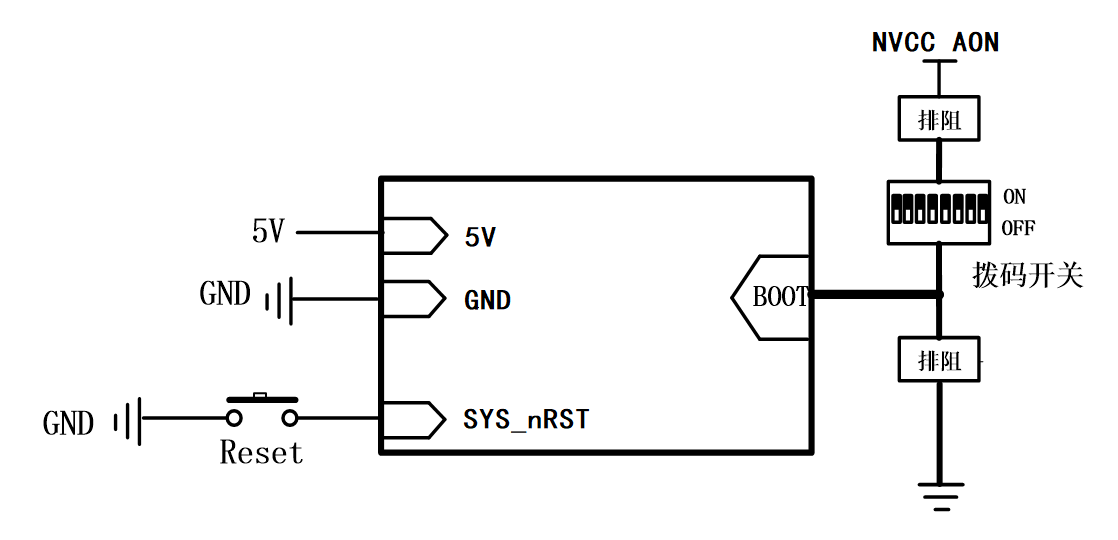
The FET-MX93xx-C / FET-MX91xx-C SoMs integrate the power supplies, reset-monitoring circuitry, and storage circuitry into one compact module, so the external circuitry required is minimal. A minimum system needs only a 5V power supply, a reset button, and boot configuration to run, as shown below.
In most cases, however, we recommend connecting a few external devices beyond the minimum system — for example, a debug serial port so you can view console output, and a reserved OTG port so you can flash the system. Once these are in place, add the functions you need on top, following the SoM’s default interface pin definitions provided by Forlinx.
1.2 SoM Power Supply
The power supply pins are listed in the table below:
Pin |
Signal |
Input/Output |
Description |
Notes |
|---|---|---|---|---|
R97 |
VSYS_5V |
Input |
SoM main power supply (typ. 5V) |
Main power input of the SoM. We recommend placing a filter capacitor close to the SoM’s VSYS_5V input pins to provide a more stable power input. Reference value: 100 nF. Pay attention to the capacitor’s voltage rating. |
R98 |
VSYS_5V |
Input |
SoM main power supply (typ. 5V) |
|
R99 |
VSYS_5V |
Input |
SoM main power supply (typ. 5V) |
|
R100 |
VSYS_5V |
Input |
SoM main power supply (typ. 5V) |
|
L76 |
USB1_VBUS_3V3 |
Input |
USB1 controller power supply |
|
L80 |
USB2_VBUS_3V3 |
Input |
USB2 controller power supply |
|
L37 |
NVCC_AON |
Output |
3.3V output from the SoM |
Used to control the carrier board’s power-up sequence |
R10 |
VSD_3V3 |
Output |
3.3V output from the SoM |
Used to power the TF (microSD) card on the carrier board |
1.3 Power-Up Sequence
The FET-MX93xx-C / FET-MX91xx-C V1.3 SoM is powered by a 5V DC supply; we recommend using a stable 5V source. After power-up, the SoM outputs an enable signal. When designing your carrier board, we strongly recommend following the development kit design and using the SoM’s NVCC_AON output as the carrier board’s power-up enable, so that the SoM always powers up strictly before the carrier board. Otherwise, latch-up may occur: the carrier board can back-feed current into the SoM, preventing the device from booting — or even causing irreversible damage to the processor.
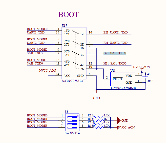
1.4 BOOT Configuration Circuit
The boot configuration pins are listed in the table below:
Pin |
Signal |
Input/Output |
Description |
Notes |
|---|---|---|---|---|
L15 |
E21_UART1_TXD |
Input at power-on reset |
BOOT mode config 0 |
We recommend using the SoM’s NVCC_AON output for the BOOT signal pull-ups. All four BOOT_MODE[3:0] pins on the SoM already have pull-up or pull-down resistors. See the pin multiplexing table for details. |
L19 |
F21_UART2_TXD |
Input at power-on reset |
BOOT mode config 1 |
|
L3 |
G21_SAI1_TXFS |
Input at power-on reset |
BOOT mode config 2 |
|
L7 |
H21_SAI1_TXD0 |
Input at power-on reset |
BOOT mode config 3 |
The mapping between the boot configuration pin levels and the boot method is shown below:
BOOT_MODE[3:0] |
BOOT CORE |
Function |
|---|---|---|
0000 |
Cortex-A55 |
Boot from Internal Fuses |
0001 |
Cortex-A55 |
Serial Download (USB1/2) |
0010 |
Cortex-A55 |
uSDHC1 8-bit eMMC 5.1 |
0011 |
Cortex-A55 |
uSDHC2 4-bit SD 3.0 |
0100 |
Cortex-A55 |
FlexSPI Serial NOR |
0101 |
Cortex-A55 |
FlexSPI Serial NAND 2K |
0110 |
Cortex-A55 |
Reserved |
0111 |
Cortex-A55 |
Reserved |
1000 |
Cortex-M33 |
LPB: Boot from Internal Fuses |
1001 |
Cortex-M33 |
LPB: Serial Downloader (USB1) |
1010 |
Cortex-M33 |
LPB: uSDHC1 8-bit 1.8 V eMMC 5.1 |
1011 |
Cortex-M33 |
LPB: uSDHC2 4-bit SD 3.0 |
1100 |
Cortex-M33 |
LPB: FlexSPI Serial NOR |
1101 |
Cortex-M33 |
LPB: FlexSPI Serial NAND 2K |
1110 |
Cortex-M33 |
Reserved |
1111 |
Cortex-M33 |
Reserved |
The boot options currently supported by the SoM are: OTG flashing on the Cortex-A55, eMMC boot on the Cortex-A55, and TF card boot on the Cortex-A55.
The boot configuration pins have on-board pull-ups/pull-downs; the default state is 0010, i.e. eMMC boot on the Cortex-A55.
Note: 1 = high level, 0 = low level.
The reference circuit is shown in the figure below.
1.5 Reset Signals
The SoM has two reset-related pins, SYS_nRST and POR_B, both active low. SYS_nRST is the SoM’s power-on reset signal, and POR_B is the CPU reset signal.
1.6 Power On/Off (ON/OFF)
The ONOFF pin controls the SoM’s power on/off. Taking this pin as a button example: in ON mode (the SoM’s normal operating state), pressing the button triggers an interrupt, and a long press forces the SoM to shut down. In OFF mode (the SoM’s power-off state), pressing the button switches the internal power-management state back to ON mode.
Note: When SYS_nRST, POR_B, or ONOFF is not used, leave the pin floating — do not add pull-up or pull-down resistors.
1.7 Flashing the System
To make debugging easier, when designing your own carrier board we recommend implementing at least one of the two flashing methods: TF card flashing or OTG flashing.
1.7.1 TF Card Flashing
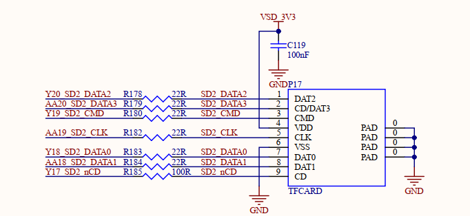
The FET-MX93xx-C / FET-MX91xx-C SoM uses the SD2 signal group for TF card flashing. After negotiation between the TF card and the SoM, this group’s voltage domain can switch between 3.3V and 1.8V. We recommend using the SoM’s VSD_3V3 output to power the TF card. Avoid powering the TF card separately: VSD_3V3 is managed centrally by the SoM, which guarantees that soft and hard resets work correctly in high-speed card mode without damaging the TF card.
Notes:
The bus pull-up resistors are already implemented on the SoM — do not add pull-ups to this bus on the carrier board;
TF cards are hot-pluggable; provide ESD protection;
SD signals must be length-matched;
If you do not implement the TF card flashing circuit and instead reuse this signal group as ordinary GPIOs, its voltage domain stays at 3.3V and will not switch to 1.8V.
The reference design is shown in the figure below.
1.7.2 OTG Flashing
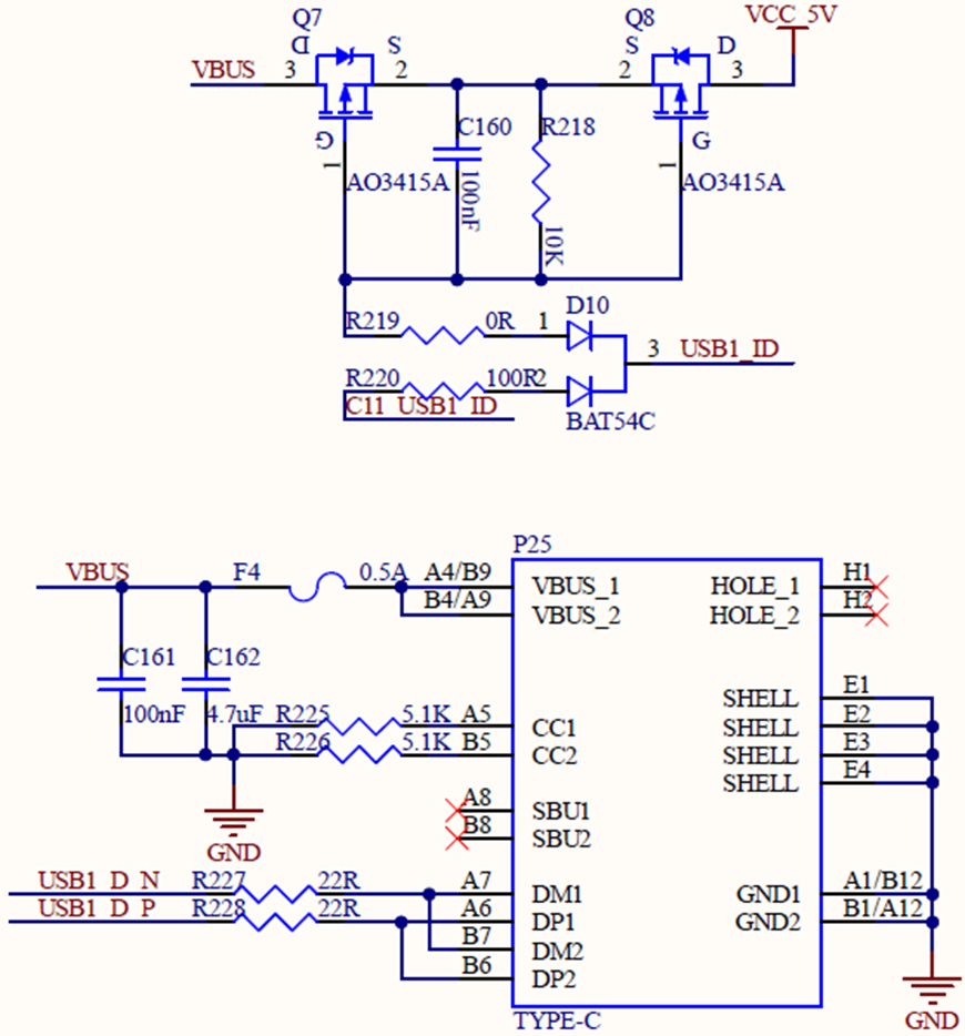
The SoM’s native USB 2.0 port USB1 supports flashing the system over USB. The USB function is enabled only when a voltage is detected on USB1_VBUS_3V3 at the connector.
Notes:
The OTG port is a pluggable connector; choose suitable ESD protection devices;
The USB data lines require 90Ω differential impedance;
The USB data lines must be length-matched;
The USB1_VBUS_3V3 pin voltage is 3.3V — make sure the voltage division is handled correctly.
1.8 Debug Serial Ports
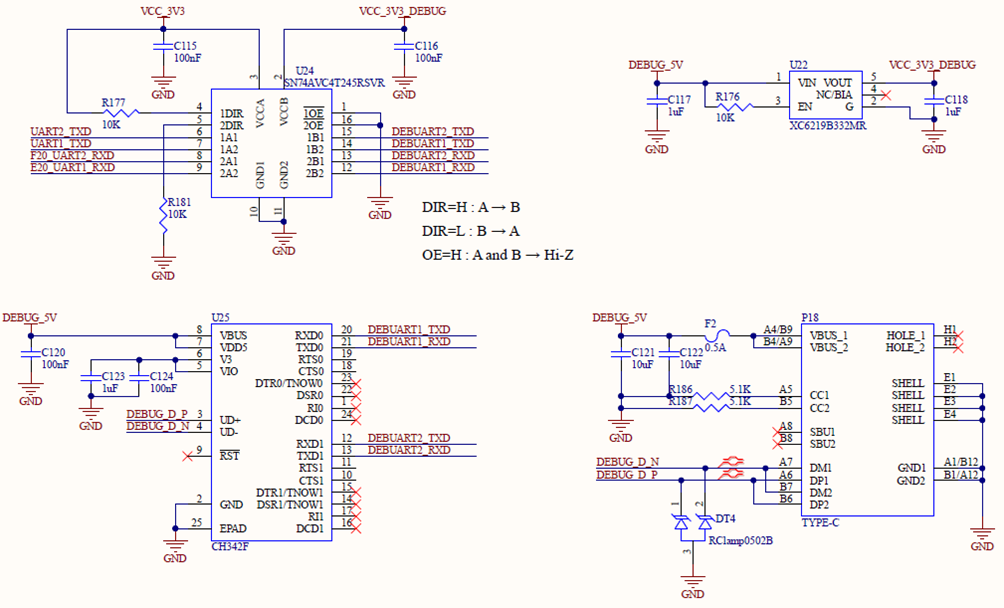
The SoM provides two debug serial ports: UART1 for debugging the Cortex-A55 cores and UART2 for debugging the Cortex-M33 core, both at 3.3V signal levels. To make debugging easier later, please bring these debug serial ports out on your carrier board. As a reference, you can convert the two UARTs into one USB bus for convenient debugging.
The reference design is shown in the figure below.
1.9 Interface Design
Note: The interface counts below are maximum values. Interfaces are multiplexed with one another; to finalize a specific scheme, refer to the Pin Multiplexing Table we provide.
1.9.1 I2C
The FET-MX93xx-C / FET-MX91xx-C SoM supports up to 8 I2C buses;
Standard mode runs at 100 Kbit/s; fast mode runs at 400 Kbit/s;
I2C is an open-drain interface and must have pull-up resistors;
Devices sharing one bus must not have conflicting I2C addresses;
I2C2 is already used and pulled up on the SoM; the on-module devices use addresses 0x25 and 0x51;
Do not multiplex I2C2 to other functions on the carrier board, and do not add pull-ups to I2C2 on the carrier board.
1.9.2 SPI
The FET-MX93xx-C / FET-MX91xx-C SoM supports up to 7 SPI buses;
The maximum data rate is 52 Mbit/s; master and slave modes are configurable;
SPI selects devices on a bus via chip-select signals, and each device’s mode can be configured independently.
1.9.3 USB (2.0/4G)
The FET-MX93xx-C / FET-MX91xx-C SoM supports up to 2 USB 2.0 ports;
USB_VBUS_3V3 is the USB port power-detection signal: when a USB device’s power is shorted, this signal notifies the CPU to shut down the USB function. The signal level is 3.3V;
By default, the 4G module uses the USB 2.0 protocol;
USB signals can be expanded through a hub chip.
1.9.4 SD (SDIO)
The FET-MX93xx-C / FET-MX91xx-C SoM supports up to 3 SDHC controllers. SDHC1 supports 8-bit eMMC 5.1 and is used by the SoM itself, so it is not available to the carrier board; SDHC2 supports 4-bit SD card 3.0; SDHC3 supports 4-bit SDIO 3.0;
SD2 is the SD (TF) card interface, 4-bit, supporting 1.8V/3.3V mode switching. We recommend using the SoM’s VSD_3V3 output to power the SD (TF) card;
SDIO signals must not have their voltage levels changed through level-shifter chips.
1.9.5 DSI, LVDS, RGB
The FET-MX93xx-C SoM supports up to 1 × 4-lane DSI at up to 1.5 Gbps; the FET-MX91xx-C does not support DSI;
The FET-MX93xx-C SoM supports up to 1 × LVDS in 4-lane mode; the FET-MX91xx-C does not support LVDS;
The FET-MX93xx-C / FET-MX91xx-C SoMs support up to 1 × LCD, with a maximum resolution of 1366×768@60 or 1280×800@60.
1.9.6 ENET & TSN
The FET-MX93xx-C / FET-MX91xx-C SoM supports up to 2 RGMII ports, one of which supports TSN;
TSN is enabled on ENET by default;
The two PHY chips are attached to different MDIO buses by default, so their addresses may be identical; the default address is 001;
Note that the RGMII pin voltage level is 1.8V;
Note that pull-up resistors are required on the MDC and MDIO signals.
1.9.7 CAN
The FET-MX93xx-C / FET-MX91xx-C SoM supports up to 2 CAN buses;
Both the CAN FD protocol (up to 5 Mbps) and the CAN 2.0B protocol are supported;
The development kit uses isolated CAN transceivers by default.
1.9.8 UART, RS-485
The FET-MX93xx-C / FET-MX91xx-C SoM supports up to 8 UARTs with a maximum baud rate of 5 Mbps;
4 UARTs default to 3.3V levels; each can be used as a 3-wire or 5-wire serial port and can go through level shifters;
UART1 serves as the debug port for the Cortex-A55, and UART2 as the debug port for the Cortex-M33;
To reduce common-mode interference, the ground signals of different RS-485 devices may be connected together.
1.9.9 CSI
The FET-MX93xx-C / FET-MX91xx-C SoM supports up to 1 × 2-lane MIPI camera at up to 1.5 Gbps.
1.9.10 Audio
The FET-MX93xx-C / FET-MX91xx-C SoM supports up to 3 SAI (synchronous audio interface) ports;
Full-duplex serial interfaces with frame sync are supported, including I2S, AC97, TDM, and codec/DSP interfaces;
By default, an I2S interface is used to connect the codec chip.
1.9.11 GPIO
The FET-MX93xx-C / FET-MX91xx-C SoM supports up to 94 GPIOs, all with interrupt capability;
Pay attention to the voltage level of each GPIO pin; refer to the hardware manual for details.
1.9.12 Other Functions
The FET-MX93xx-C / FET-MX91xx-C SoM supports up to 2 PWM channels;
The FET-MX93xx-C / FET-MX91xx-C SoM supports up to 1 QSPI (already used by the SoM, connected to a 16 MB NOR flash);
The FET-MX93xx-C / FET-MX91xx-C SoM supports up to 1 JTAG port;
The FET-MX93xx-C / FET-MX91xx-C SoM supports up to 2 I3C buses;
The FET-MX93xx-C / FET-MX91xx-C SoM supports up to 4 ADC channels.
2. PCB Design
2.1 General Design Rules
Unless otherwise required, route single-ended signals with an impedance of 50Ω ±10%;
Route clock and high-speed signals at least 250 mil away from board edges, and at least 500 mil away from switching-regulator inductors and MOSFETs;
Route clocks adjacent to a complete ground plane; add ground guarding where necessary;
Do not route other signals near or underneath crystals;
Keep reset signals away from clock lines and switching power-supply circuits;
Apply the 3W rule between different buses, and between interference sources and sensitive signals, wherever possible;
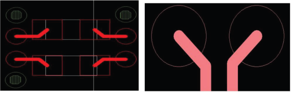
For differential pairs, make left and right bends consistent, and keep entries into pads and vias symmetric, as shown in the figure below;
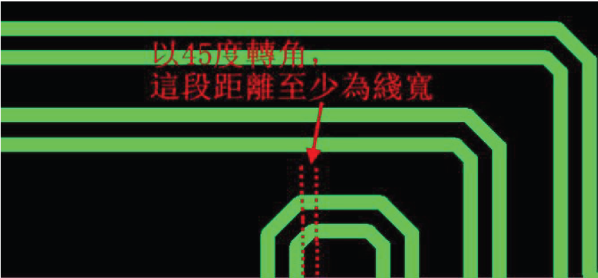
When length-tuning (serpentining) traces, keep the width of each turning segment at least equal to the trace width. If this is unavoidable, make sure the trace width and spacing at the corners still meet the rules, as shown in the figure below;
Place filter capacitors at the chip’s power input, as close to the pins as possible.
2.2 I2C
The bus topology is shown below;
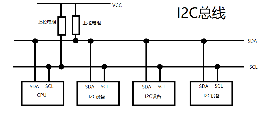
Place I2C pull-up resistors as close to the source as possible;
If an I2C device on the bus is sensitive to glitches (even small glitches can trigger it falsely, and once such a device is attached it can disrupt more sensitive devices on the same bus), add an RC filter at the device end. The capacitor should be in the pF range, and the bus carrying that device should be routed as short as possible — guard the clock line where possible.
2.3 USB (2.0/4G)
USB 3.0 ports use point-to-point routing. U3_TX_DP and U3_TX_DN require AC coupling; place the coupling capacitors close to the receiver end;
USB 2.0 has only the USB_DP and USB_DM signals and does not require AC coupling;
USB signals must be routed differentially with an impedance of 90Ω ±10%;
Keep USB trace lengths within 150 mm, and intra-pair length mismatch within 0.12 mm;
Place ESD protection devices no more than 12 mm from the USB connector, and the common-mode choke no more than 25 mm from it.
2.4 SDIO
Route SDIO signals as single-ended traces with an impedance of 50Ω ±10%;
Apply length matching to SDIO interface signals, keeping the mismatch within 0.25 mm;
Keep routing as short as possible; place series termination resistors close to the driving end.
2.5 DSI, LVDS, HDMI
Route DSI signals differentially with an impedance of 100Ω ±10%;
Route LVDS signals differentially with an impedance of 100Ω ±10%, and reserve footprints for 100Ω resistors between the differential pairs;
Route HDMI signals differentially with an impedance of 100Ω ±10%, and apply length matching.
2.6 ENET
When multiple PHY chips are attached to the MDIO bus, use daisy-chain (series) routing — do not branch the trace;
The RGMII interface consists of transmit signals, receive signals, and control signals; control each group’s impedance at 50Ω ±10%;
Keep transmit and receive signal trace lengths within 100 mm, with intra-group length mismatch within 2.54 mm;
Reserve a capacitor to ground on the clock line to make later debugging easier;
Route the MDI interface differentially with an impedance of 100Ω ±10%;
Keep intra-pair mismatch of the MDI pairs within 0.12 mm;
Keep the power inductor connected to the chip’s internal DC-DC close to the chip to minimize the current loop, and keep the ground return path complete;
Place the reserved series resistors on data lines close to the source;
Place protection devices on the transformer side — between the transformer and the PHY, close to the transformer.
2.7 CAN
Route CAN differentially and reserve footprints for 120Ω termination resistors;
Reserve a ground signal at the connector.
2.8 RS-485
Route RS-485 differentially and reserve footprints for 120Ω termination resistors;
The RS-485 bus transmits in half-duplex mode, so transmit/receive control is required;
Reserve a ground signal at the connector.
2.9 CSI
Route CSI signals differentially with an impedance of 100Ω ±10%.
2.10 Audio
The connection between the SoM and the codec is digital; use single-ended routing;
Reserve filter capacitors on the I2S clock signals;
Audio signals are analog and must be isolated from digital signals; add ground guarding where necessary to keep the reference ground intact.
2.11 PCIe
PCIe ports use point-to-point routing with AC coupling; place the coupling capacitors close to the transmit end;
Route PCIe transmit/receive data signals differentially with an impedance of 85Ω ±15%;
Route the PCIe clock signal differentially with an impedance of 100Ω ±10%;
Keep the total differential pair length within 300 mm, intra-pair mismatch within 0.12 mm, and length mismatch between same-direction differential pairs within 180 mm; keep pair-to-pair spacing no less than 0.3 mm.
3. Troubleshooting Common Interface Issues
3.1 General Troubleshooting Steps
If your carrier board follows a Forlinx reference design, first make sure the function chip matches the reference schematic exactly. A different chip may require porting its driver;
If the chip matches the reference but function verification fails, check the function chip’s power supply, reset, and clock one by one;
Cross-test to determine whether the problem is on the SoM or on the carrier board;
Check whether pin voltage levels are matched and whether the data signals have output;
Check for soldering defects: cold joints, solder bridges, missing components, or wrongly placed components;
Measure whether the signals’ idle state is normal;
Confirm that the pin multiplexing configuration is correct.
3.2 Failure to Boot
Besides power and reset, check whether the PWR_EN signal is normal;
Confirm whether pull-up/pull-down circuits were added to the boot-configuration pins in the carrier board design.
3.3 I2C
I2C is open-drain — first confirm that pull-up resistors are present;
Check whether devices attached to the same I2C bus have conflicting addresses;
Measure the signal waveforms: is the idle state high, and are the waveforms normal during data transmission?
If the waveform rises too slowly, decrease the pull-up resistance; if the low level is too high, increase the pull-up resistance;
Use the i2c-tools to check whether devices are attached to the bus:
i2cdetect -l        # Detect how many I2C buses exist on the system
i2cdetect -r -y 2   # Detect devices attached to I2C bus 2
3.4 SPI
Do not cross-connect MISO and MOSI;
Confirm that the chip-select signal is connected;
Confirm that both communicating devices are configured with the same SPI mode;
Measure whether the clock and data outputs are normal.
3.5 USB (2.0/4G)
Check whether the USB_VBUS_3V3 signal is at 3.3V;
The USB positive and negative data signals must not be cross-connected — verify that the USB signals are wired correctly.
3.6 SDIO
The SD2 interface’s pin voltage depends on the transfer speed: it defaults to 3.3V and switches to 1.8V in high-speed mode;
SDIO signals must not have their voltage levels changed through level-shifter chips;
If the speed does not meet requirements, besides checking pin voltage levels, also confirm whether the SDIO bus is length-matched;
For the SDIO bus, check the clock output first.
3.7 LVDS
Check whether the LVDS display’s output mode matches the panel (VESA vs. JEIDA);
Measure whether the clock and data outputs are normal.
3.8 ENET
Confirm that the communication interface between the PHY chip and the MAC matches, and that length matching has been applied;
Check whether the MDIO bus is pulled up and whether the waveform is normal; do not branch MDIO routing;
Confirm that the precision resistors meet the requirements;
If the speed does not meet requirements, check each power rail and whether the reference ground is complete;
Check whether the network transformer’s center taps are connected correctly;
Check whether PHY chips on the same bus have conflicting addresses, and whether the addresses match the software configuration;
Check whether the MDI data lines are length-matched and whether the impedance meets the requirements.
3.9 CAN
When multiple devices are on the CAN bus, confirm that devices at both ends have 120Ω matching resistors;
If a CAN device cannot communicate, try connecting the device’s reference ground to reduce common-mode interference.
3.10 UART
The serial transmit and receive signals must be cross-connected;
Confirm that the serial terminal tool is configured correctly (e.g., baud rate);
Measure whether the data output is normal.
3.11 RS-485
When multiple devices are on the RS-485 bus, confirm that devices at both ends have 120Ω matching resistors;
If an RS-485 device cannot communicate, try connecting the devices’ reference grounds to reduce common-mode interference;
RS-485 transmits in half-duplex mode, and some RS-485 chips require a transmit/receive control signal — confirm that the chip’s driver has been added.
3.12 Audio
If the system cannot detect the audio chip, check whether communication on the I2C bus is working;
If the chip mounts normally but there is no audio output, first check whether the I2S data waveform is being output correctly, then check the audio output path.
3.13 GPIO
When selecting a GPIO, confirm whether the pin is a boot-configuration pin. If it is, do not add pull-up/pull-down circuits to it at power-on — or add a buffer chip instead.