User’s Hardware Manual_V2.0
Document classification: □ Top secret □ Secret □ Internal information ■ Open
Copyright
The copyright of this manual belongs to Baoding Folinx Embedded Technology Co., Ltd. Without the written permission of our company, no organizations or individuals have the right to copy, distribute, or reproduce any part of this manual in any form, and violators will be held legally responsible.
Forlinx adheres to copyrights of all graphics and texts used in all publications in original or license-free forms.
The drivers and utilities used for the components are subject to the copyrights of the respective manufacturers. The license conditions of the respective manufacturer are to be adhered to. Related license expenses for the operating system and applications should be calculated/declared separately by the related party or its representatives.
Revision History
Date |
User Manual Version |
SoM Version |
Carrier Board Version |
Revision History |
|---|---|---|---|---|
22/07/2020 |
V1.0 |
V1.3 |
V1.1 |
OK1043A/1046A-C2_User’s Hardware Manual Initial Version. |
05/11/2020 |
V1.1 |
V1.3 |
V1.1 |
Modification of PCIE parameters in SoM interface resource. |
20/05/2021 |
V1.2 |
V1.3/V2.0 |
V1.1 |
1. Adding the ordering information of SoM V2.0; |
27/07/2021 |
V1.3 |
V1.3/V2.0 |
V1.1 |
Modifying boot configuration section description. |
30/092022 |
V2.0 |
V1.5/V2.2 |
V2.1 |
1. Correction of SATA parameters in the interface resources of the SoM; |
Overview
This manual is designed to help users quickly familiarize themselves with the product, understand interface functions and configuration, and primarily discusses the interface functions of the development board, interface introductions, product power consumption, and troubleshooting issues that may arise during use. Some commands were commented to make it easier for you to understand (adequate and practical for the purpose). For information on pin function multiplexing, hardware troubleshooting methods, etc., please refer to Forlinx’s “ FET1046-C2 Pin Multiplexing Comparison Table”.
There are total four chapters:
Chapter 1. is CPU overview, briefly introducing its performance and applications;
Chapter 2. is comprehensive introduction to the SoM, including connector pins explanations and function introductions;
Chapter 3. is comprehensive introduction to the development board, divided into multiple chapters, including both hardware principles and simple design ideas;
Chapter 4. mainly describes the board’s power consumption performance and other considerations.
A description of some of the symbols and formats associated with this manual:
Format |
Meaning |
|---|---|
Note |
Note or information that requires special attention, be sure to read carefully. |
📚 |
Relevant notes on the test chapters. |
🛤️ |
Indicates the related path. |
1. NXP QorIQ LS104xA Description
The QorIQ® LS104xA processor is a quad - core 64 - bit ARM® processor launched by NXP for embedded networks. The LS1023A (dual - core version) and LS104xA (quad - core version) can provide a performance of over 10 Gbps through a flexible I/O package that supports fanless design. This SoC is a solution specifically designed for small - form - factor network and industrial applications. It has optimized the BOM for cost - effective low - end PCB, reduced power supply costs, and adopted a single - clock design. The new 0.9V versions of the LS104xA and LS1023A can offer additional power consumption savings for wireless LAN and Power over Ethernet systems. The new 23x23 package supports a pin - compatible design and can be expanded to the LS1046A (quad - core A72 processor). The QorIQ LS104xA can enhance the performance of dual - core 32 - bit ARM products and continues the consistent I/O flexibility of the QorIQ series. It integrates the QUICC Engine® and continues to provide seamless support for HDLC, TDM, or Profibus.
The CPU of the FET104xA - C SoM uses the LS1043AXE8QQB and LS1046AXE8T1A. The following is the application processing block diagram of the LS1043A and LS1046A:
LS1043A Block Diagram
LS1046A Block Diagram
For more details about the LS104xA series please visit the official NXP website: https://www.nxp.com/cn/products/processors-and-microcontrollers/arm-based-processors-and-mcus/qoriq-layerscape-arm-processors/qoriq-layerscape-1043a-and-1023a-multicore-communications-processors:LS1043A
2. FET104xA-C SoM Description
2.1 FET104xA SoM Appearance
FET1043A-C Front
FET1046A-C Front
2.2 FET104xA-C SoM Dimension Diagram
The dimensions of the FET104x-C SoM are as follows:
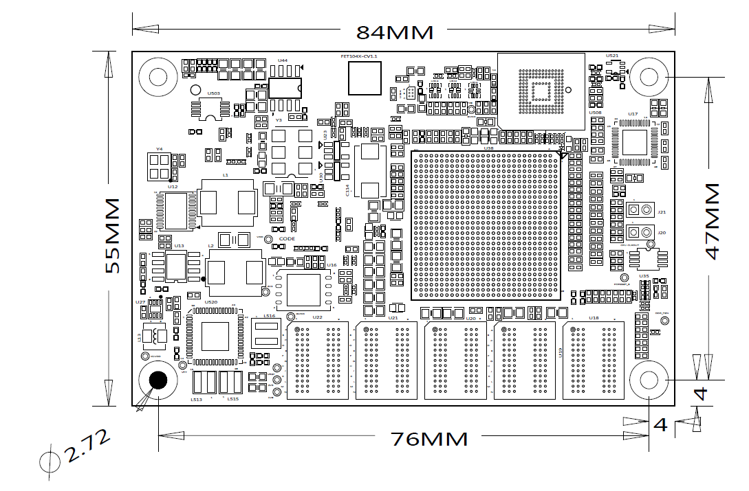
Structure size: 84mm×55mm
Plate making process: 2mm thickness, 12-layer immersion gold PCB.
Connectors: Double-row 0.5mm pitch, 220pin board-to-board connectors. Refer to Appendix for the connector dimension diagram.
Four mounting holes with a diameter of 2.7mm are reserved at the four corners of the SoM. The overall structure of the SoM complies with the COM Express® Mini Type 10 standard.
2.3 Performance Parameters
2.3.1 System Main Frequency
Name |
Specification |
Description |
|||
|---|---|---|---|---|---|
Minimum |
Typical |
Maximum |
Unit |
||
Main Frequency |
— |
— |
1600 |
MHz |
LS1046 maximum 1.8G |
RTC clock |
— |
32.768 |
— |
KHz |
— |
DDR clock |
650 |
— |
1600 |
MT/s |
— |
SerDes reference clock |
100 |
— |
156.25 |
MHz |
— |
2.3.2 Power Parameter
Parameter |
Pin Number |
Specification |
Description |
|||
|---|---|---|---|---|---|---|
Minimum |
Typical |
Maximum |
Unit |
|||
Main Power Supply Voltage |
VCC_12V |
9 |
12 |
15 |
V |
— |
2.3.3 Operating Environment
Parameter |
Specification |
Description |
||||
|---|---|---|---|---|---|---|
Minimum |
Typical |
Maximum |
Unit |
|||
Operating temperature |
Operating Environment |
-40 |
25 |
+80* |
℃ |
Industrial-grade |
Storage Environment |
-40 |
25 |
+125 |
℃ |
||
Humidity |
Operating Environment |
10 |
— |
90 |
%RH |
No condensation |
Storage Environment |
5 |
— |
95 |
%RH |
Note: The maximum operating environment temperature of FET1046A-C SoM is 75 ℃.
2.3.4 SoM Interface Speed
Parameter |
Specification |
Description |
|||
|---|---|---|---|---|---|
Minimum |
Typical |
Maximum |
Unit |
||
Serial Port Communication Speed |
— |
115200 |
— |
bps |
— |
IIC Communication Speed |
— |
100 |
400 |
Kbps |
— |
SD/MMC/SDIO |
— |
— |
104 |
Mbps |
— |
USB interface speed |
— |
— |
5 |
Gbps |
— |
2.4 SoM Interface Speed
Function |
FET1043 Quantity |
FET1046 Quantity |
Parameter |
|---|---|---|---|
QSGMII |
≤1 |
≤1 |
Maximum communication rate 5G |
SGMII |
≤4 |
≤5 |
The maximum supported speed is 2.5G |
RGMII |
≤2 |
≤2 |
The maximum supported speed is 1G. |
UART |
≤4 |
≤4 |
Supports 2 x DUART or 4 x UART |
IIC |
≤2 |
≤2 |
|
USB3.0 |
≤3 |
≤3 |
The maximum supported speed is 5G. |
XFI |
≤1 |
≤2 |
The maximum supported speed is 10G, up to 2 x. |
eSDHC |
≤1 |
≤1 |
Supports SD3.0 EMMC4.5, shared with eMMC on the SoM. |
PCIE2.0 |
≤3 |
- |
The maximum supported speed is 5G. |
PCIE3.0 |
- |
≤3 |
The maximum supported speed is 8G. |
SATA3.0 |
≤1 |
≤1 |
The maximum supported speed is 6G. |
JTAG |
1 |
1 |
Support NXP’s official CodeWarrior TAP debugger. |
Note: The parameters in the table are the theoretical values of hardware design or CPU.
2.5 FET104xA SoM Pins Definition
2.5.1 FET104xA SoM Pins Schematic
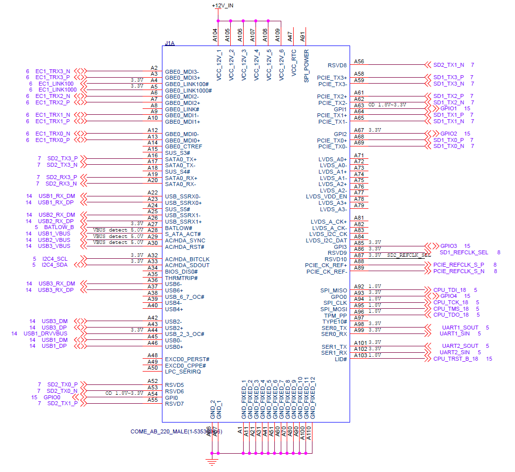
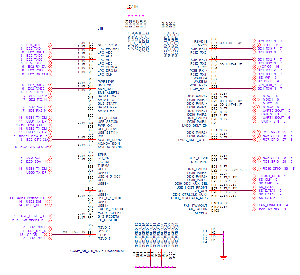
2.5.2 FET104xA SoM Pin Functions Description
Note1:
Num ——SoM connector pin no.:
Ball —— CPU pin ball no.
GPIO ——CPU pin general I/O port serial number
Vol —— Pin signal level
NC——The pins are not connected.
Note2:
Signal Name——SoM connector network name
Pin Description—— SoM Pin Signal Descriptions
Default function-All pin functions of the SoM are specified according to the “default function” in the table below. Please do not modify it, otherwise it may be delivered from the factory.
Drive conflict. If you have any questions, please contact our sales or technical support in a timely manner.
Note3: The default function indicates that this signal only supports the LS1046A chip and the LS1043A CPU does not have this pin.
Table 1 Connector Interface (Odd) Pin Definitions A
NUM |
BALL |
Signal Name |
GPIO |
VOL |
Pin Description |
Default Function |
|---|---|---|---|---|---|---|
A1 |
- |
GND |
- |
- |
Ground |
GND |
A2 |
- |
EC1_TRX3_N |
- |
1.1V |
YT8521S TR3- |
EC1_TRX3_N |
A3 |
- |
EC1_TRX3_P |
- |
1.1V |
YT8521S TR3+ |
EC1_TRX3_P |
A4 |
- |
EC1_LINK100 |
- |
1.5V |
Meaningless, default output low |
EC1_LINK100 |
A5 |
- |
EC1_LINK1000 |
- |
1.5V |
YT8521S Gigabit indication |
EC1_LINK1000 |
A6 |
- |
EC1_TRX2_N |
- |
1.1V |
YT8521S TR2- |
EC1_TRX2_N |
A7 |
- |
EC1_TRX2_P |
- |
1.1V |
YT8521S TR2+ |
EC1_TRX2_P |
A8 |
- |
NC |
- |
- |
- |
NC |
A9 |
- |
EC1_TRX1_N |
- |
1.1V |
YT8521S TR1- |
EC1_TRX1_N |
A10 |
- |
EC1_TRX1_P |
- |
1.1V |
YT8521S TR1+ |
EC1_TRX1_P |
A11 |
- |
GND |
- |
- |
Ground |
GND |
A12 |
- |
EC1_TRX0_N |
- |
1.1V |
YT8521S TR0- |
EC1_TRX0_N |
A13 |
- |
EC1_TRX0_P |
- |
1.1V |
YT8521S TR0+ |
EC1_TRX0_P |
A14 |
- |
NC |
- |
- |
- |
NC |
A15 |
- |
NC |
- |
- |
- |
NC |
A16 |
AD19 |
SD2_TX3_P |
- |
1.35V |
1046:SD2_TX3_P |
|
1043:SD1_TX3_P |
||||||
A17 |
AE19 |
SD2_TX3_N |
- |
1.35V |
1046:SD2_TX3_N |
|
1043:SD1_TX3_N |
||||||
A18 |
- |
NC |
- |
- |
- |
NC |
A19 |
AG19 |
SD2_RX3_P |
- |
1.0V |
1046:SD2_RX3_P |
|
1043:SD1_RX3_P |
||||||
A20 |
AH19 |
SD2_RX3_N |
- |
1.0V |
1046:SD2_RX3_N |
|
1043:SD1_RX3_N |
||||||
A21 |
- |
GND |
- |
- |
Ground |
GND |
A22 |
E4 |
USB1_RX_DM |
- |
1.0V |
USB1_RX- |
USB1_RX_DM |
A23 |
E3 |
USB1_RX_DP |
- |
1.0V |
USB1_RX+ |
USB1_RX_DP |
A24 |
- |
NC |
- |
- |
- |
NC |
A25 |
C4 |
USB2_RX_DM |
- |
1.0V |
USB2_RX- |
USB2_RX_DM |
A26 |
C3 |
USB2_RX_DP |
- |
1.0V |
USB2_RX+ |
USB2_RX_DP |
A27 |
J4 |
BATLOW_B |
GPIO1_24 |
3.3V |
General IO |
GPIO1_24 |
A28 |
E7 |
USB1_VBUS |
- |
5.25V |
USB1 VBUS |
USB1_VBUS |
A29 |
C7 |
USB2_VBUS |
- |
5.25V |
USB2 VBUS |
USB2_VBUS |
A30 |
A7 |
USB3_VBUS |
- |
5.25V |
USB3 VBUS |
USB3_VBUS |
A31 |
- |
GND |
- |
- |
Ground |
GND |
A32 |
M3 |
I2C4_SCL |
GPIO4_12 |
3.3V |
I2C4 SCL |
I2C4_SCL |
A33 |
N3 |
I2C4_SDA |
GPIO4_13 |
3.3V |
I2C4 SDA |
I2C4_SDA |
A34 |
- |
NC |
- |
- |
- |
NC |
A35 |
- |
NC |
- |
- |
- |
NC |
A36 |
A4 |
USB3_RX_DM |
- |
1.0V |
USB3_RX- |
USB3_RX_DM |
A37 |
A3 |
USB3_RX_DP |
- |
1.0V |
USB3_RX+ |
USB3_RX_DP |
A38 |
- |
NC |
- |
- |
- |
NC |
A39 |
- |
NC |
- |
- |
- |
NC |
A40 |
- |
NC |
- |
- |
- |
NC |
A41 |
- |
GND |
- |
- |
Ground |
GND |
A42 |
A6 |
USB3_DM |
- |
3.3V |
USB3_D- |
USB3_DM |
A43 |
B6 |
USB3_DP |
- |
3.3V |
USB3_D+ |
USB3_DP |
A44 |
H6 |
USB1_DRVVBUS |
GPIO4_29 |
3.3V |
USB1 DRVVBUS |
USB1_DRVVBUS |
A45 |
E6 |
USB1_DM |
- |
3.3V |
USB1_D- |
USB1_DM |
A46 |
F6 |
USB1_DP |
- |
3.3V |
USB1_D+ |
USB1_DP |
A47 |
- |
NC |
- |
- |
- |
NC |
A48 |
- |
NC |
- |
- |
- |
NC |
A49 |
- |
NC |
- |
- |
- |
NC |
A50 |
- |
NC |
- |
- |
- |
NC |
A51 |
- |
GND |
- |
- |
Ground |
GND |
A52 |
AD15 |
SD2_TX0_P* |
- |
1.35V |
1046:SD2_TX0_P |
|
1043:NC |
||||||
A53 |
AE15 |
SD2_TX0_N* |
- |
1.35V |
1046:SD2_TX0_N |
|
1043:NC |
||||||
A54 |
R3 |
GPIO0 |
GPIO2_01 |
1.8V |
General IO |
GPIO0 |
A55 |
AD16 |
SD2_TX1_P |
- |
1.35V |
1046:SD2_TX1_P |
|
1043:SD1_TX2_P |
||||||
A56 |
AE16 |
SD2_TX1_N |
- |
1.35V |
1046:SD2_TX1_N |
|
1043:SD1_TX2_N |
||||||
A57 |
- |
GND |
- |
- |
Ground |
GND |
A58 |
AD11 |
SD1_TX3_P* |
- |
1.35V |
1046:SD1_TX3_P |
|
1043:NC |
||||||
A59 |
AE11 |
SD1_TX3_N* |
- |
1.35V |
1046:SD1_TX3_P |
|
1043:NC |
||||||
A60 |
- |
GND |
- |
- |
Ground |
GND |
A61 |
AD10 |
SD1_TX2_P |
- |
1.35V |
1046:SD1_TX2_P |
|
1043:SD1_TX1_P |
||||||
A62 |
AE10 |
SD1_TX2_N |
- |
1.35V |
1046:SD1_TX2_N |
|
1043:SD1_TX1_N |
||||||
A63 |
T3 |
GPIO1 |
GPIO2_02 |
1.8V |
General IO |
GPIO1 |
A64 |
AD8 |
SD1_TX1_P* |
- |
1.35V |
1046:SD1_TX1_P |
|
1043:NC |
||||||
A65 |
AE8 |
SD1_TX1_N* |
- |
1.35V |
1046:SD1_TX1_N |
|
1043:NC |
||||||
A66 |
- |
GND |
- |
- |
Ground |
GND |
A67 |
V1 |
GPIO2 |
GPIO3_13 |
1.8V |
General IO |
GPIO2 |
A68 |
AD6 |
SD1_TX0_P |
- |
1.35V |
1046:SD1_TX0_P |
|
1043:SD1_TX0_P |
||||||
A69 |
AE6 |
SD1_TX0_N |
- |
1.35V |
1046:SD1_TX0_N |
|
1043:SD1_TX0_N |
||||||
A70 |
- |
NC |
- |
- |
- |
NC |
A71 |
- |
NC |
- |
- |
- |
NC |
A72 |
- |
NC |
- |
- |
- |
NC |
A73 |
- |
NC |
- |
- |
- |
NC |
A74 |
- |
NC |
- |
- |
- |
NC |
A75 |
- |
NC |
- |
- |
- |
NC |
A76 |
- |
NC |
- |
- |
- |
NC |
A77 |
- |
NC |
- |
- |
- |
NC |
A78 |
- |
NC |
- |
- |
- |
NC |
A79 |
- |
NC |
- |
- |
- |
NC |
A80 |
- |
GND |
- |
- |
Ground |
GND |
A81 |
- |
NC |
- |
- |
- |
NC |
A82 |
- |
NC |
- |
- |
- |
NC |
A83 |
- |
NC |
- |
- |
- |
NC |
A84 |
- |
NC |
- |
- |
- |
NC |
A85 |
C20 |
GPIO3 |
GPIO2_12 |
1.8V |
General IO |
GPIO3 |
A86 |
- |
SD1_REFCLK_SEL |
- |
3.3V |
SERDES1 clock selection |
SD1_REFCLK_SEL |
A87 |
- |
NC |
- |
- |
- |
NC |
A88 |
- |
PCIE_REFCLK_S_P |
- |
3.3V |
PCIE_REFCLK+ |
PCIE_REFCLK_S_P |
A89 |
- |
PCIE_REFCLK_S_N |
- |
3.3V |
PCIE_REFCLK- |
PCIE_REFCLK_S_N |
A90 |
- |
GND |
- |
- |
Ground |
GND |
A91 |
- |
NC |
- |
- |
- |
NC |
A92 |
G17 |
CPU_TDI_18 |
- |
1.8V |
JTAG_TDI |
CPU_TDI_18 |
A93 |
B18 |
GPIO4 |
GPIO2_13 |
1.8V |
General IO |
GPIO4 |
A94 |
E18 |
CPU_TCK_18 |
- |
1.8V |
JTAG_TCK |
CPU_TCK_18 |
A95 |
G18 |
CPU_TMS_18 |
- |
1.8V |
JTAG_TMS |
CPU_TMS_18 |
A96 |
E20 |
CPU_TDO_18 |
- |
1.8V |
JTAG_TDO |
CPU_TDO_18 |
A97 |
- |
NC |
- |
- |
- |
NC |
A98 |
H1 |
UART1_SOUT |
GPIO1_15 |
3.3V |
UART1_TX |
UART1_SOUT |
A99 |
H2 |
UART1_SIN |
GPIO1_17 |
3.3V |
UART1_RX |
UART1_SIN |
A100 |
- |
GND |
- |
- |
Ground |
GND |
A101 |
L2 |
UART2_SOUT |
GPIO1_16 |
3.3V |
UART2_TX |
UART2_SOUT |
A102 |
K1 |
UART2_SIN |
GPIO1_18 |
3.3V |
UART2_RX |
UART2_SIN |
A103 |
- |
CPU_TRST_B_18 |
- |
1.8V |
JTAG_RST |
CPU_TRST_B_18 |
A104 |
- |
VCC_12V |
- |
12V |
SoM power supply |
VCC_12V |
A105 |
- |
VCC_12V |
- |
12V |
SoM power supply |
VCC_12V |
A106 |
- |
VCC_12V |
- |
12V |
SoM power supply |
VCC_12V |
A107 |
- |
VCC_12V |
- |
12V |
SoM power supply |
VCC_12V |
A108 |
- |
VCC_12V |
- |
12V |
SoM power supply |
VCC_12V |
A109 |
- |
VCC_12V |
- |
12V |
SoM power supply |
VCC_12V |
A110 |
- |
GND |
- |
- |
Ground |
GND |
Table 2 Connector interface pin definition B
NUM |
BALL |
Signal Name |
GPIO |
VOL |
Pin Description |
Deflaut Function |
|---|---|---|---|---|---|---|
B1 |
- |
GND |
- |
- |
Ground |
GND |
B2 |
- |
EC1_ACT |
- |
1.5V |
YT8521S effective indication |
EC1_ACT |
B3 |
AE4 |
EC2_TXD1 |
GPIO3_17 |
1.8V |
RGMII TXD1 |
EC2_TXD1 |
B4 |
AE1 |
EC2_RXD1 |
GPIO3_24 |
1.8V |
RGMII RXD1 |
EC2_RXD1 |
B5 |
AF3 |
EC2_TXD0 |
GPIO3_18 |
1.8V |
RGMII TXD0 |
EC2_TXD0 |
B6 |
AE3 |
EC2_TXD2 |
GPIO3_16 |
1.8V |
RGMII TXD2 |
EC2_TXD2 |
B7 |
AD3 |
EC2_TXD3 |
GPIO3_15 |
1.8V |
RGMII TXD3 |
EC2_TXD3 |
B8 |
AF1 |
EC2_RX_DV |
GPIO3_27 |
1.8V |
RGMII RX_DV |
EC2_RX_DV |
B9 |
AE2 |
EC2_RXD0 |
GPIO3_25 |
1.8V |
RGMII RXD0 |
EC2_RXD0 |
B10 |
AC1 |
EC2_RX_CLK |
GPIO3_26 |
1.8V |
RGMII RX_CLK |
EC2_RX_CLK |
B11 |
- |
GND |
- |
- |
Ground |
GND |
B12 |
- |
NC |
- |
- |
- |
NC |
B13 |
AD1 |
EC2_RXD2 |
GPIO3_23 |
1.8V |
RGMII RXD2 |
EC2_RXD2 |
B14 |
AC2 |
EC2_RXD3 |
GPIO3_22 |
1.8V |
RGMII RXD3 |
EC2_RXD3 |
B15 |
AG3 |
EC2_TXEN |
GPIO3_19 |
1.8V |
RGMII TXEN |
EC2_TXEN |
B16 |
AD18 |
SD2_TX2_P* |
- |
1.35V |
1046:SD2_TX2_P |
|
1043:NC |
||||||
B17 |
AE18 |
SD2_TX2_N* |
- |
1.35V |
1046:SD2_TX2_N |
|
1043:NC |
||||||
B18 |
- |
NC |
- |
- |
- |
NC |
B19 |
AG18 |
SD2_RX2_P* |
- |
1.0V |
1046:SD2_RX2_P |
|
1043:NC |
||||||
B20 |
AH18 |
SD2_RX2_N* |
- |
1.0V |
1046:SD2_RX2_N |
|
1043:NC |
||||||
B21 |
- |
GND |
- |
- |
Ground |
GND |
B22 |
F2 |
USB1_TX_DM |
- |
1.0V |
USB1 TX- |
USB1_TX_DM |
B23 |
F1 |
USB1_TX_DP |
- |
1.0V |
USB1 TX+ |
USB1_TX_DP |
B24 |
- |
PWR_OK |
- |
Carrier board power-on normal signal |
PWR_OK |
|
B25 |
D2 |
USB2_TX_DM |
- |
1.0V |
USB2 TX- |
USB2_TX_DM |
B26 |
D1 |
USB2_TX_DP |
- |
1.0V |
USB2 TX+ |
USB2_TX_DP |
B27 |
F10 |
RESET_REQ_B_18 |
- |
1.8V |
CPU reset output |
RESET_REQ_B_18 |
B28 |
AC4 |
EC2_GTX_CLK |
GPIO3_20 |
1.8V |
RGMII GTX_CLK |
EC2_GTX_CLK |
B29 |
- |
NC |
- |
- |
- |
NC |
B30 |
AG4 |
EC2_GTX_CLK125 |
GPIO3_21 |
1.8V |
RGMII CLK125 |
EC2_GTX_CLK125 |
B31 |
- |
GND |
- |
- |
Ground |
GND |
B32 |
- |
NC |
- |
- |
- |
NC |
B33 |
L4 |
I2C3_SCL |
GPIO4_10 |
3.3V |
I2C3 SCL |
I2C3_SCL |
B34 |
M4 |
I2C3_SDA |
GPIO4_11 |
3.3V |
I2C3 SDA |
I2C3_SDA |
B35 |
- |
NC |
- |
- |
- |
NC |
B36 |
B2 |
USB3_TX_DM |
- |
1.0V |
USB3 TX- |
USB3_TX_DM |
B37 |
B1 |
USB3_TX_DP |
- |
1.0V |
USB3 TX+ |
USB3_TX_DP |
B38 |
- |
NC |
- |
- |
- |
NC |
B39 |
- |
NC |
- |
- |
- |
NC |
B40 |
- |
NC |
- |
- |
- |
NC |
B41 |
- |
GND |
- |
- |
Ground |
GND |
B42 |
- |
NC |
- |
- |
- |
NC |
B43 |
- |
NC |
- |
- |
- |
NC |
B44 |
G6 |
USB1_PWRFAULT |
GPIO4_30 |
3.3V |
USB power error detection |
USB1_PWRFAULT |
B45 |
C6 |
USB2_DM |
- |
3.3V |
USB2_D- |
USB2_DM |
B46 |
D6 |
USB2_DP |
- |
3.3V |
USB2_D+ |
USB2_DP |
B47 |
- |
NC |
- |
- |
- |
NC |
B48 |
- |
NC |
- |
- |
- |
NC |
B49 |
- |
SYS_RESET_B |
- |
3.3V |
System reset input |
SYS_RESET_B |
B50 |
- |
CB_RESET_B |
- |
3.3V |
System reset output |
CB_RESET_B |
B51 |
- |
GND |
- |
- |
Ground |
GND |
B52 |
AG15 |
SD2_RX0_P* |
- |
1.0V |
1046:SD2_RX0_P |
|
1043:NC |
||||||
B53 |
AH15 |
SD2_RX0_N* |
- |
1.0V |
1046:SD2_RX0_N |
|
1043:NC |
||||||
B54 |
D17 |
GPIO5 |
GPIO2_14 |
1.8V |
General IO |
GPIO5 |
B55 |
AG16 |
SD2_RX1_P |
- |
1.0V |
1046:SD2_RX1_P |
|
1043:SD1_RX2_P |
||||||
B56 |
AH16 |
SD2_RX1_N |
- |
1.0V |
1046:SD2_RX1_N |
|
1043:SD1_RX2_N |
||||||
B57 |
E17 |
GPIO6 |
GPIO2_15 |
1.8V |
General IO |
GPIO6 |
B58 |
AG11 |
SD1_RX3_P* |
- |
1.0V |
1046:SD1_RX3_P |
|
1043:NC |
||||||
B59 |
AH11 |
SD1_RX3_N* |
- |
1.0V |
1046:SD1_RX3_N |
|
1043:NC |
||||||
B60 |
- |
GND |
- |
- |
Ground |
GND |
B61 |
AG10 |
SD1_RX2_P |
- |
1.0V |
1046:SD1_RX2_P |
|
1043:SD1_RX1_P |
||||||
B62 |
AH10 |
SD1_RX2_N |
- |
1.0V |
1046:SD1_RX2_N |
|
1043:SD1_RX1_N |
||||||
B63 |
W3 |
GPIO7 |
GPIO1_31 |
1.8V |
General IO |
GPIO7 |
B64 |
AG8 |
SD1_RX1_P* |
- |
1.0V |
1046:SD1_RX1_P |
|
1043:NC |
||||||
B65 |
AH8 |
SD1_RX1_N* |
- |
1.0V |
1046:SD1_RX1_N |
|
1043:NC |
||||||
B66 |
L3 |
SD_WP |
GPIO4_03 |
3.3V |
SD card write protection |
SD_WP |
B67 |
K3 |
SD_CD_B |
GPIO4_02 |
3.3V |
SD plug detection |
SD_CD_B |
B68 |
AG6 |
SD1_RX0_P |
- |
1.0V |
1046:SD1_RX0_P |
|
1043:SD1_RX0_P |
||||||
B69 |
AH6 |
SD1_RX0_N |
- |
1.0V |
1046:SD1_RX0_N |
|
1043:SD1_RX0_N |
||||||
B70 |
- |
GND |
- |
- |
Ground |
GND |
B71 |
AG2 |
MDC1 |
GPIO3_00 |
1.8V |
MDC1 |
MDC1 |
B72 |
AF2 |
MDIO1 |
GPIO3_01 |
1.8V |
MDIO1 |
MDIO1 |
B73 |
AH4 |
MDC2 |
GPIO4_00 |
1.8V |
MDC2 |
MDC2 |
B74 |
AH3 |
MDIO2 |
GPIO4_01 |
1.8V |
MDIO2 |
MDIO2 |
B75 |
J2 |
UART3_SOUT |
GPIO1_19 |
3.3V |
UART3 TX |
UART3_SOUT |
B76 |
J1 |
UART3_SIN |
GPIO1_21 |
3.3V |
UART3 RX |
UART3_SIN |
B77 |
L1 |
UART4_SOUT |
GPIO1_20 |
3.3V |
UART4 TX |
UART4_SOUT |
B78 |
M2 |
UART4_SIN |
GPIO1_22 |
3.3V |
UART4 RX |
UART4_SIN |
B79 |
- |
NC |
- |
- |
- |
NC |
B80 |
- |
GND |
- |
- |
Ground |
GND |
B81 |
J5 |
IRQ5_GPIO1_25 |
GPIO1_25 |
3.3V |
General IO |
GPIO1_25 |
B82 |
K5 |
IRQ6_GPIO1_26 |
GPIO1_26 |
3.3V |
General IO |
GPIO1_26 |
B83 |
L5 |
IRQ7_GPIO1_27 |
GPIO1_27 |
3.3V |
Interrupt input |
IRQ7_GPIO1_27 |
B84 |
- |
NC |
- |
- |
- |
NC |
B85 |
- |
NC |
- |
- |
- |
NC |
B86 |
- |
NC |
- |
- |
- |
NC |
B87 |
- |
NC |
- |
- |
- |
NC |
B88 |
M5 |
IRQ8_GPIO1_28 |
GPIO1_28 |
3.3V |
Interrupt input |
IRQ8_GPIO1_28 |
B89 |
N5 |
IRQ9_GPIO1_29 |
GPIO1_29 |
3.3V |
General IO |
GPIO1_29 |
B90 |
- |
GND |
- |
- |
Ground |
GND |
B91 |
P4 |
IRQ10_GPIO1_30 |
GPIO1_30 |
3.3V |
Interrupt input |
IRQ10_GPIO1_30 |
B92 |
- |
NC |
- |
- |
- |
NC |
B93 |
A16 |
BOOT_SEL0 |
- |
1.8V |
Enable the options |
BOOT_SEL0 |
B94 |
P3 |
SD_CLK |
GPIO2_09 |
1.8V/3.3V |
SD CLK |
SD_CLK |
B95 |
P2 |
SD_CMD |
GPIO2_04 |
1.8V/3.3V |
SD CMD |
SD_CMD |
B96 |
P1 |
SD_DATA0 |
GPIO2_05 |
1.8V/3.3V |
SD DATA0 |
SD_DATA0 |
B97 |
R2 |
SD_DATA1 |
GPIO2_06 |
1.8V/3.3V |
SD DATA1 |
SD_DATA1 |
B98 |
R1 |
SD_DATA2 |
GPIO2_07 |
1.8V/3.3V |
SD DATA2 |
SD_DATA2 |
B99 |
T1 |
SD_DATA3 |
GPIO2_08 |
1.8V/3.3V |
SD DATA3 |
SD_DATA3 |
B100 |
- |
GND |
- |
- |
Ground |
GND |
B101 |
A19 |
FAN_PWMOUT |
GPIO2_10 |
1.8V |
Fan control |
FAN_PWMOUT |
B102 |
D20 |
FAN_TACHIN |
GPIO2_11 |
1.8V |
Fan speed detection |
FAN_TACHIN |
B103 |
- |
NC |
- |
- |
- |
NC |
B104 |
- |
VCC_12V |
- |
12V |
SoM power supply |
VCC_12V |
B105 |
- |
VCC_12V |
- |
12V |
SoM power supply |
VCC_12V |
B106 |
- |
VCC_12V |
- |
12V |
SoM power supply |
VCC_12V |
B107 |
- |
VCC_12V |
- |
12V |
SoM power supply |
VCC_12V |
B108 |
- |
VCC_12V |
- |
12V |
SoM power supply |
VCC_12V |
B109 |
- |
VCC_12V |
- |
12V |
SoM power supply |
VCC_12V |
B110 |
- |
GND |
- |
- |
Ground |
GND |
3. OK104xA-C2 Development Platform Description
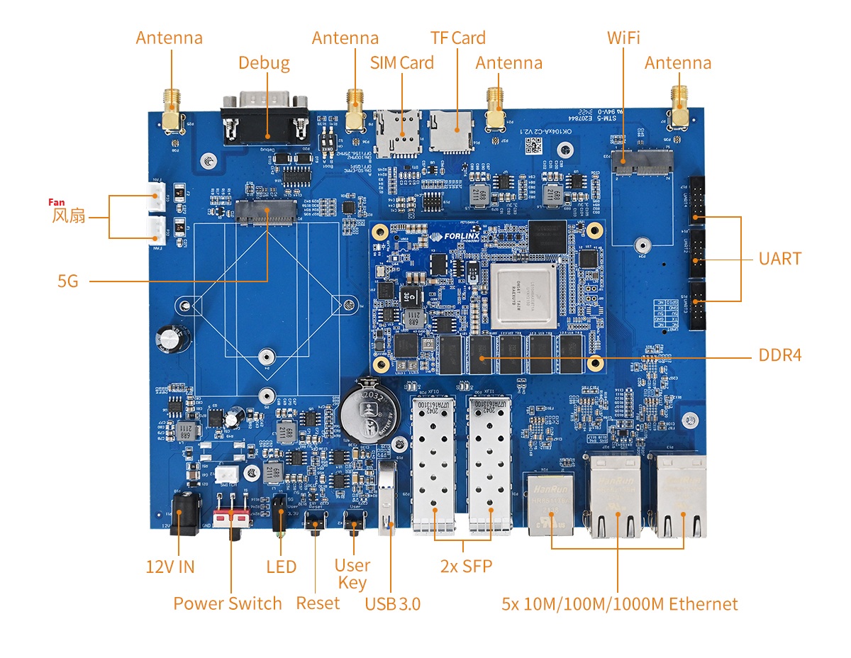
3.1 OK104xA-C2 Development Board Interface Diagram
The Forlinx OK104xA-C2 development platform consists of a System on Module (SoM) and a carrier board connected by connectors. The carrier board is compatible with both the FET1043A-C and FET1046A-C SoMs. Therefore, the term “OK104xA-C2” is displayed on the PCB silkscreen and is also used as the name of the development board in this document. This term serves as a general reference for the CPU series with which this product is compatible. The main interfaces of the OK104xA - C2 development board are shown in the following figure:
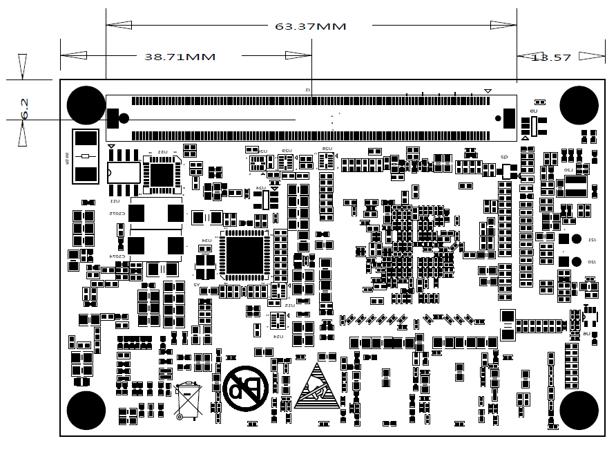
3.2 OK104xA-C2 Development Board Dimension Diagram
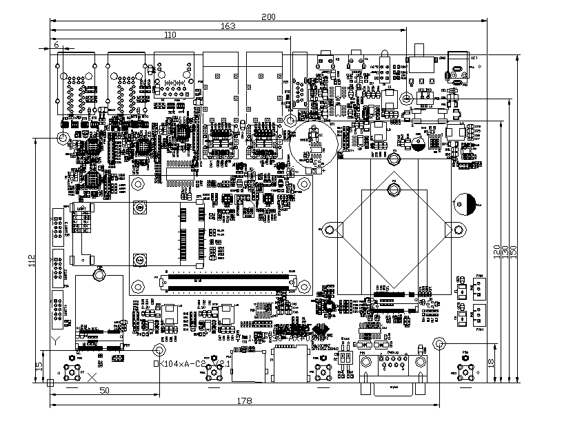
PCB Size: 200mm × 150mm
Plate making process: thickness 2mm, 6-layer PCB.
Power supply voltage: DC 12V.
Fixing hole diameter: 3.2mm
3.3 Carrier Board Naming Rules
A - B - C + D E F : G - H
Field |
Field Description |
Value |
Description |
|
|---|---|---|---|---|
A |
Product Line Identification |
OK |
Forlinx Embedded carrier board/development board |
|
TCU |
Forlinx embedded charging control unit |
|||
- |
Segment Identification |
- |
When the first digit of the CPU value is a letter, |
|
B |
CPU |
2440 |
S3C2440 |
|
2416 |
S3C2416 |
|||
6410 |
S3C6410 |
|||
210 |
S5pV210 |
|||
335x |
AM335x |
|||
MX6x |
The x stands for a carrier board that is compatible with multiple CPU, |
|||
i.MX6Q/QP/DP/DL/D |
||||
MX6UL |
i.MX6UL |
|||
xx18 |
S5p4418 / S5p6818 |
|||
5718 |
AM5718 |
|||
1052 |
i.MX RT1052 |
|||
1061 |
i.MX RT1061 |
|||
1012A |
LS1012A |
|||
104xA |
LS1043A/LS1046A |
|||
A40i |
A40i |
|||
T3 |
T3 |
|||
MX8MM |
i.MX8M Mini |
|||
MX8MQ |
i.MX8MQ |
|||
MX8MPQ |
i.MX8MPQ |
|||
T507 |
T507 |
|||
1028A |
LS1028A |
|||
3519A |
Hi3519 |
|||
3399 |
RK3399/3399K |
|||
3568 |
RK3568/3568J |
|||
G2LD |
RZ/G2LD |
|||
6254 |
AM6254 |
|||
- |
Segment Identification |
- |
Parameter segment sign |
|
C |
Connection |
Sx |
Edge Connector |
|
Dx |
Pin connection |
|||
Cx |
Board-to-board Connector |
|||
Gx |
Golden-finger |
|||
Note: The content of x is null or 2 ~ N to |
||||
+ |
Segment Identification |
+ |
The configuration parameter section follows this identifier. |
|
D |
Type Identification |
M |
Carrier board (Note: carrier board identification M, not filled by default.) |
|
E |
Expansion boards (including Bluetooth boards, Wi - Fi boards, |
|||
L |
Light board |
|||
D |
Display board |
|||
K |
Key board |
|||
P |
Power board |
|||
E |
Operating temperature |
C |
0 to 70℃ commercial-grade |
|
E |
-20 to 85℃ extended commercial grade |
|||
I |
-40 to 85℃ industrial level |
|||
A |
-40 to 125℃ vehicle level |
|||
F |
PCB Version |
10 |
V1.0 |
|
xx |
Vx.x |
|||
: |
Separator |
: |
It’s followed by the manufacture’s internal identification. |
|
G |
Connector origin |
0 |
Chinese-made connector |
|
1 |
Imported connector |
|||
N |
No differentiation/no connector |
|||
- |
Connector |
- |
Grade mark connector |
|
H |
Grade Identification |
PC |
Prototype sample |
|
Blank |
Mass Production |
|||
SC |
Special-purpose use: According to the customer’s special |
3.4 Carrier Board Resources
Function |
Quantity |
Parameter 5 |
|---|---|---|
RGMII |
2 |
10/10/1000Mbps adaptive,RJ-45 interface |
SGMII3 |
3 |
10/10/1000Mbps adaptive,RJ-45 interface |
USB 3.0 |
1 |
The maximum supported speed is 5G. |
TF Card |
1 |
|
Mini PCIE1 |
1 |
External SATA hard drive |
PCIE X12 |
2 |
The maximum supported speed is 5G. |
RTC |
1 |
On-board CR2032 battery |
UART |
3 |
TTL level |
RS232 |
1 |
Debugging serial port |
JTAG |
1 |
Support NXP’s official CodeWarrior TAP debugger. |
SFP4 |
2 |
Supports XFI 10G |
Note:
The LS1043A can only be used as a mini PCIE;
Only the LS1046A supports it;
The LS1043A only supports 2 x, which are P26 and P27 on the carrier board;
The LS1043A only supports 1 x, which is P28 on the carrier board;
The parameters in the table are the hardware design or CPU theoretical values.
3.5 OK104xA- C2 Carrier Board Description
Note: The component UID with “_DNP” mark in the diagram below represents it is not soldered by default.
3.5.1 Carrier Board Power
The carrier board is powered by a DC 12V supply, which is introduced through the DC - 005 socket (P10) or the 2 - pin 5.08mm terminal (P11). The power - on switch of the whole board is realized by using S1 to control the Q3 MOSFET, which can reduce the oxidation of the switch contacts caused by the large current at the moment of power - on and prolong the service life of the switch.
Discharge resistors are added before and after the switch to ensure that the capacitor voltage can be quickly discharged after the switch is turned off.
3.5.2 Reset
The tactile switch K1 on the left side of the development board can reset the CPU and peripheral chips when pressed.
RESET_REQ_B_18 is a reset request signal output by the CPU. When the CPU has an abnormal situation (such as when the watchdog is triggered), this signal will be pulled low. When the CPU startup process is abnormal, the RESET_REQ_B_18 signal should be delayed for a specific period before resetting the CPU. This delay allows sufficient time for JTAG to control the CPU. Therefore, it is advisable to include a reset delay chip similar to the component labeled U13 in the reference design.
There are a total of 4 reset - related pins led out from the SoM, namely CPU_TRST_B_18, RESET_REQ_B_18, SYS_RESET_B, and CB_RESET_B.
Name |
Function |
|---|---|
CPU_TRST_B_18 |
JTAG reset, reset CPU and CB _ RESET _ B at the same time. |
RESET_REQ_B_18 |
CPU abnormal reset output. |
SYS_RESET_B |
Reset the input of the SoM and reset CB_RESET_B at the same time. |
CB_RESET_B |
SoM reset output, used to reset the carrier board peripheral chip. |
3.5.3 Boot Configuration
The LS104xA CPU uses RCW (Reset configuration word) to select the boot option, while the FET104xA-C2 SoM defaults to booting from QSPI NOR Flash (with the carrier board BOO_SEL0 floated).
Boot Configuration Schematic
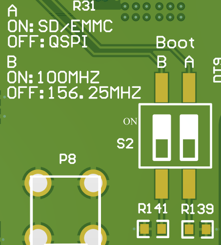
PCB silk screen
S2 DIP switch description:
PCB silk screen |
Name |
Function |
|---|---|---|
A |
BOOT_SEL0 |
OFF(1):QSPI start (default) |
ON(0):SD/EMMC start |
||
B |
SD1_REFCLK_SEL |
OFF(1): 156.25Mhz reference clock (deflaut) |
ON(0): 100MHz reference clock |
SD1_REFCLK_SEL controls the reference clock of SD1_REFCLK2 (CPU ball numbers are AA8 and AB8). Please select this clock source according to the specific configuration of SerDes.
In the SD/EMMC boot mode, the SD card insertion detection pin SD_CD_B controls whether to boot from the SD card or the EMMC. After inserting the SD card, the SD_CD_B pin is pulled low, and the CPU boots from the SD card. When the SD card is not inserted, the SD_CD_B pin is pulled high by default, and the CPU boots from the on - board EMMC of the SoM.
Signal |
Status |
Mode |
|---|---|---|
SD_CD_B |
0 |
SD Card |
1 |
EMMC |
3.5.4 Serial Port
The P20 is a standard 9-pin RS-232 interface using a DB9 male connector to connect to a PC. If the computer does not have an RS-232 serial port, you can use the USB to serial port module to export the serial port.
P14, P15 and P17 are UART2, UART3 and UART4 3.3V TTL serial ports respectively.
Note: To facilitate subsequent debugging, please lead out this debugging serial port when designing the carrier board by yourself.
3.5.5 PCIE Interface
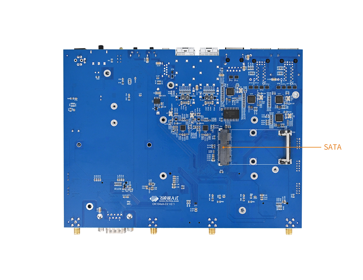
There are 3 x PCIE interfaces on the OK104xA-C2 carrier board by default, namely the mini PCIE interface P21, the PCIE X1 interfaces P2 and P23. The FET1043A-C SoM only supports the P21 interface.
The P21 mini PCIE interface on the LS1046A can be configured as either a PCIE or an mSATA interface. (In the mSATA interface, the polarity of RX is opposite to that in the PCIE standard. The software supports the change, and it can be designed according to the mini PCIE standard.)
The P2 interface supports both USB3.0 and PCIEX1 protocols and can be connected to 5G modules from Quectel.
The P23 interface can be connected to a PCIE - interface Wi - Fi module.
Since the SATA hard drive, 5G module, and Wi - Fi module have high power consumption, their power is supplied by a separate DCDC.
Note: PCIE devices do not support hot - plugging, and the power of the corresponding modules should be powered on simultaneously with the carrier board.
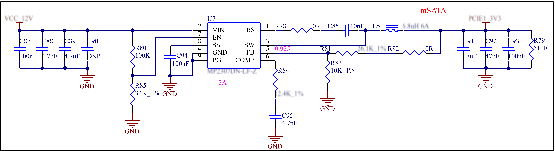
Note:
Please keep the PCIE reset pin to ensure that the PCIE device is effectively reset every time the power is turned on;
Change the PCIE clock chip to RC19004A100GNL.
3.5.6 TF Card
The development board is equipped with a self - ejecting TF card socket, which supports the SD UHS - 1 speed mode.
Note:
The level matching of the pull - up on the TF data line has been completed by the SoM, and the carrier board does not need to perform pull - up processing;
When designing, please note that the TF card insertion and removal detection status affects the boot item. See Section 3.5.3 Boot Configuration for details.
3.5.7 RGMII
There are 2 x RGMII - type Gigabit PHY interfaces on the OK104xA-C2 development board, both using the YT8521SH chip. One PHY is on the SoM and is directly led out to the RJ45 on the carrier board, and the other is on the carrier board. The RGMII signals are connected to U10.
Note:
The address 00000 of the YT8521SH is the broadcast address. Please use it with caution during configuration;
When designing the PCB, ensure that the PHY chip has a complete reference ground;
If the PHY chip connected to the RGMII on the carrier board is removed in hardware, the YT8521SH chip connected to the RGMII on the SoM will not work properly. Please try to avoid such a configuration. If it must be used in this way, please contact Forlinx for software modification.
3.5.8 JTAG Simulation Debugging Interface
There is a JTAG debugging interface (P19) on the carrier board, which is convenient for you to simulate and debug LS104xA.
The reset signal CPU_TRST_B_18 cannot be left floating. Whether the JTAG function is used or not, this pin needs to be pulled up to 1.8V.
3.5.9 SGMII Interface
There are 3 x SGMII PHY, which are respectively connected to the YT8521SH chips of U18, U19, and U20. Among them, the SGMII corresponding to U19 and U20 can only be used on the LS1046A CPU, and they are left unconnected on the LS1043A.
Network interface definition:
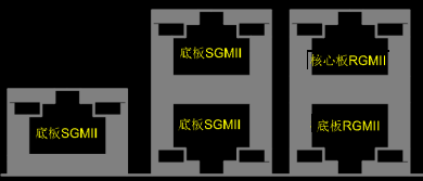
Connector |
Function |
FET1046A-C |
FET1043A-C |
|---|---|---|---|
P26 |
Carrier board SGMII |
Support |
Support |
P27 up |
Carrier board SGMII |
Support |
No support |
P27 down |
Carrier board SGMII |
Support |
No support |
P13 up |
SoM RGMII |
Support |
Support |
P13 up |
Carrier board RGMII |
Support |
Support |
3.5.10 USB3.0 Interface
USB3.0 interface, current detection VBUS power control using TPS2065. In order to eliminate interference and ensure that USB will not report errors by mistake, it is recommended to add C135 and C145 100pF capacitors.
3.5.11 SFP Interface
There are 2 x SFP interfaces. Among them, P30 is only available on the LS1046A CPU, and it is in an open - circuit state on the LS1043A CPU.
Note:
Since the theoretical maximum rate of the SPF interface can reach 10 Gbps, when drawing the PCB, the traces should be laid on the surface layer as much as possible to reduce stubs;
Since the clock buffer chip ICS8304AMI is difficult to procure, the reference clocks of U21 and U23 are now provided by active crystal oscillators;
Since the optical module may be configured through the IIC bus, the two optical modules in the development board are connected to IIC3 and IIC4 respectively, and 0Ω resistors are reserved. The default is empty welding. When configuration is required, the 0Ω resistors are welded. At the same time, it is necessary to pay attention to whether the address of the optical module will conflict with other devices on the carrier board.
3.5.12 User Key
1 x user K2 is led out from the OK104xA-C2 carrier board, and the function can be customized.
3.5.13 LED
3 x LED D1 are led out from OK104xA-C2 carrier board. Yellow is the carrier board 3.3 V power indication, green is the 5G network status indication, and red is the user-defined LED.
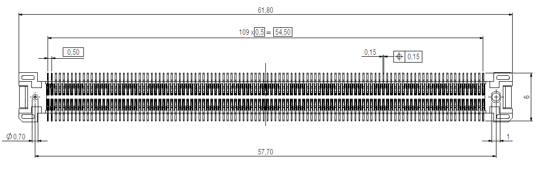
4. Connector Dimension Diagram
The specifications of the SoM connector are as follows:
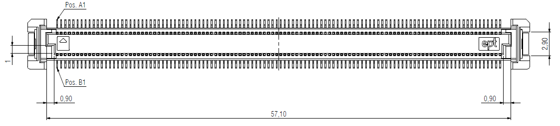
The specifications of the baseboard connector are as follows:

5. Power Consumption Measured Data
The following table shows the measured power consumption data of OK1046A when the supply voltage is 12V:
No. |
Test Item |
Development Board (A) |
SoM(A) |
|---|---|---|---|
1 |
Start instantaneous current |
1.58 |
1.27 |
2 |
Zero load current |
1.15 |
0.85 |
3 |
Full load current |
1.5 |
1.19 |
6. SoM Lmbench Test Data
Data read and write test:
Lmbench test results of V1.3 SoM:
Cache/Memory |
rd |
wr |
rdwr |
cp |
frd |
fwr |
fcp |
bzero |
bcopy |
|---|---|---|---|---|---|---|---|---|---|
L1(MB/s) |
28556 |
20928 |
19188 |
19760 |
7180 |
7178 |
6121 |
17892 |
14090 |
L2(MB/s) |
15767 |
17624 |
11256 |
9119 |
6780 |
7142 |
6522 |
11999 |
10137 |
DDR(MB/s) |
6440 |
2349 |
2387 |
1624 |
6431 |
6478 |
2726 |
6562 |
2718 |
Lmbench test results of V2.0 SoM:
Cache/Memory |
rd |
wr |
rdwr |
cp |
frd |
fwr |
fcp |
bzero |
bcopy |
|---|---|---|---|---|---|---|---|---|---|
L1(MB/s) |
28552 |
20931 |
19191 |
19392 |
7181 |
7176 |
5666 |
17345 |
14051 |
L2(MB/s) |
15767 |
17671 |
11255 |
9059 |
6757 |
7142 |
6515 |
13693 |
10067 |
DDR(MB/s) |
9858 |
3649 |
3771 |
2740 |
6432 |
7191 |
5307 |
11026 |
5306 |