User’s Hardware Manual_V1.8
Document classification: □ Top secret □ Secret □ Internal information ■ Open
Copyright
The copyright of this manual belongs to Baoding Folinx Embedded Technology Co., Ltd. Without the written permission of our company, no organizations or individuals have the right to copy, distribute, or reproduce any part of this manual in any form, and violators will be held legally responsible.
Forlinx adheres to copyrights of all graphics and texts used in all publications in original or license-free forms.
The drivers and utilities used for the components are subject to the copyrights of the respective manufacturers. The license conditions of the respective manufacturer are to be adhered to. Related license expenses for the operating system and applications should be calculated/declared separately by the related party or its representatives.
Revision History
Date |
User Manual Version |
SoM Version |
Carrier Board Version |
Revision History |
|---|---|---|---|---|
05/07/2022 |
V1.0 |
V1.1 |
V1.1 |
Initial Version |
12/01/2023 |
V1.1 |
V1.2 |
V1.2 |
Modifying the SoM model in the ordering information |
05/05/2023 |
V1.2 |
V1.2 |
V1.2 |
Improving the WIFI schematic diagram |
29/05/2023 |
V1.3 |
V1.2 |
V1.2 |
Updating BOOT configuration description |
13/06/2023 |
V1.4 |
V1.2 |
V1.2 |
Completing CPU description and minimum system schematic |
20/01/2024 |
V1.5 |
V1.2 |
V1.2 |
1. Completing the description of reset signal; |
18/03/2023 |
V1.6 |
V1.2 |
V1.2 |
Correcting the errors in the manual. |
27/08/2024 |
V1.7 |
V1.2 |
V1.2 |
1. Updating the dimension and glitch tolerance information of the SoM; |
28/01/2026 |
V1.8 |
V1.2 |
V2.2 |
The carrier board is upgraded to V2.2, and the circuit function description of the serial port and audio part is updated. |
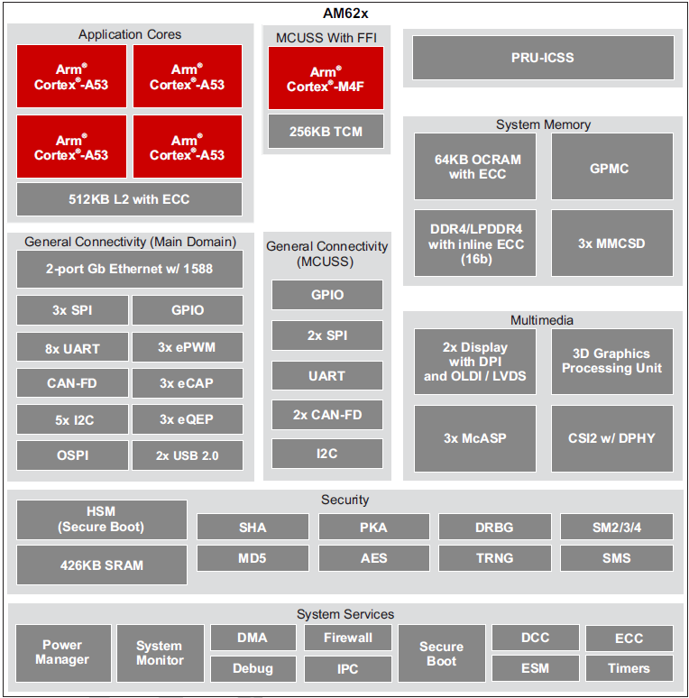
1. Introduction to AM62X
The AM62x is an extension of the Sitara™ industrial/automotive-grade heterogeneous Arm® processor family, featuring embedded 3D graphics acceleration, dual display interfaces, and a wide range of peripheral and networking options. The AM62x is built for a wide range of industrial and automotive applications. It includes up to four Arm® Cortex®-A53 cores with a 64-bit architecture, a single-core Arm® Cortex®-R5F device manager subsystem, an IMG AXE1 - 16 3D graphics module, a dual-core PRU module, and a Cortex®-M4F MCU module. The Cortex - A53x provides the powerful computing elements required for Linux applications. Linux and real - time (RT) Linux are provided through TI’s Processor SDK Linux, which is updated annually to the latest long - term support (LTS) Linux kernel, bootloader, and Yocto file system.
The AM62x has a powerful IMG AXE1 - 16 3D graphics core, suitable for HMI applications and QT acceleration, with dual display output options at a resolution of up to 2K and 60fps. Functional safety features can be enabled through the integrated Cortex - M4F and its dedicated peripherals, all of which can be isolated from the rest of the SoC. There are two external Gigabit Ethernet ports that support TSN. The additional PRU module can provide real - time I/O capabilities for customers’ own use cases. In addition, the AM62x also includes a wide range of peripheral sets to achieve system - level connectivity, such as USB, MMC/SD, camera interface, OSPI, CAN - FD, and GPMC for parallel host interfaces with external ASIC/FPGA. The AM62x supports secure boot for IP protection through a built - in HSM (Hardware Security Module) and also adopts advanced power management support for portable and power - sensitive applications.
Target Applications:
• Human - Machine Interface (HMI)
• Retail Automation
• Driver Monitoring System (DMS/OMS)/Interior Monitoring (ICM)
• Telematics Control Unit (TCU)
• 3D Point Cloud
• Vehicle-to-Infrastructure/Vehicle-to-Vehicle (V2X / V2V)
• 3D Reconfigurable Automotive Instrument Panel
• Device User Interface and Connectivity
• Medical Equipment …..
AM62x Block Diagram
2. FET62xx-C SoM Description
2.1 FET62xx-C SoM
FET62xx-C SoM Appearance:
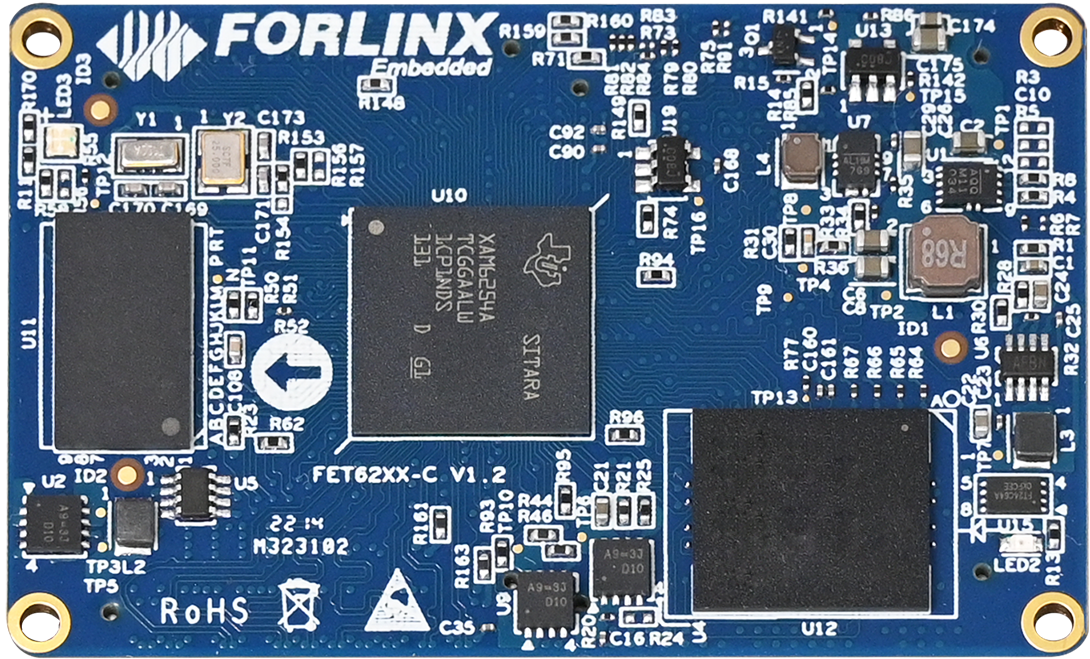
Front
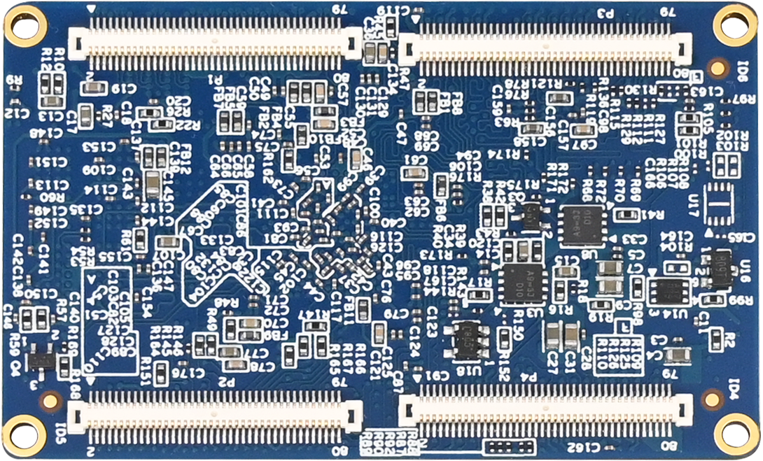
Back
2.2 FET62xx-C SoM Dimension Diagram
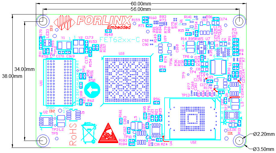
Top
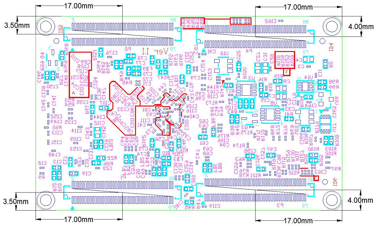
Bottom
Structure size: 60mm × 38mm, size tolerance ± 0.13mm, single side of burr tolerance ± 0.2mm.
Plate making process: 1.6mm thickness, 10-layer immersion gold PCB.
Connector: Four 0.5mm pitch, 80pin board-to-board connectors. Refer to Appendix for the connector dimension diagram.
Four mounting holes (2.2mm) are reserved at the four corners of the SoM to facilitate the installation of fixing screws and to improve the reliability of the product connection so that the product can be used in vibration environments.
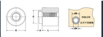
Please refer to the development board design and use SMT nuts of M2 with a length (L) of 2 mm on the carrier board. Please refer to the following figure for the specifications of the SMT nuts.
2.3 SoM Configuration Resources
2.3.1 SoM Naming Rules
A-B-C+DEFGHIJ:KL-M
Field |
Field Description |
Value |
Description |
|---|---|---|---|
A |
Product Line Identification |
FET |
Forlinx Embedded SoM |
- |
Segment Identification |
- |
When the first digit of the CPU value is a letter, connect the product line identifier to the CPU with “-”; when the first digit of the CPU value is a number, omit “-“. |
B |
CPU Name |
62xx |
AM6254, AM6231, AM6232 |
- |
Segment Identification |
- |
Parameter segment sign |
C |
Connection |
C |
Board to Board Connector |
+ |
Segment Identification |
+ |
The configuration parameter section follows this identifier. |
D |
CPU Clock |
14 |
1.4 GHz (AM6231 clock 1.0GHZ) |
E |
RAM capacity |
1G/2G |
1G/2G |
F |
Single ROM Type |
SE |
eMMC |
G |
ROM capacity |
8G |
8GB |
H |
Operating Temperature |
I |
-40 to 85℃ industrial level |
I |
Configuration No. |
A~Z |
If the D~H field values are the same for each product, then this field has the same value. It is in ascending order according to the configuration release time. |
J |
PCB Version |
12 |
V1.2 |
: |
Separator |
: |
It’s followed by the manufacture’s internal identification. |
K |
Chip Type |
A~Z |
This is the internal identification of the manufacturer and has no impact on the use. |
L |
Connector origin |
1 |
Imported connector |
2.3.2 Order Information
No. |
Specification Model |
CPU Clock |
RAM |
ROM |
Temperature Level |
|---|---|---|---|---|---|
A |
FET6254-C+141GSE8GIA12 |
1.4 GHZ |
1G |
8G |
Industrial-grade |
B |
FET6254-C+142GSE8GIB12 |
1.4 GHZ |
2G |
8G |
Industrial-grade |
A |
FET6232-C+142GSE8GIA12 |
1.4 GHZ |
2G |
8G |
Industrial-grade |
B |
FET6232-C+141GSE8GIB12 |
1.4 GHZ |
1G |
8G |
Industrial-grade |
A |
FET6231-C+101GSE8GIA12 |
1.0 GHZ |
1G |
8G |
Industrial-grade |
This table shows examples of the SoM specifications and models, but it does not cover all possible specifications. The latest specifications and models can be found in the latest product hardware manual. If the specifications you need are not listed in the table, or if you have any questions about the specifications, please visit www.forlinx.net or contact your Forlinx sales representative.
2.4 Performance Parameters
2.4.1 System Main Frequency
Name |
Specification |
Description |
|||
|---|---|---|---|---|---|
Minimum |
Typical |
Maximum |
Unit |
||
System clock Arm ® Cortex ® -53 |
— |
— |
1400 |
MHz |
— |
System clock y Arm® Cortex®-M4F |
— |
— |
400 |
MHz |
|
RTC clock |
— |
32.768 |
— |
KHz |
— |
AM6231 system clock is up to 1000MHZ
2.4.2 Power Parameter
Parameter |
Pin Number |
Specification |
Description |
|||
|---|---|---|---|---|---|---|
Minimum |
Typical |
Maximum |
Unit |
|||
Main Power Supply Voltage |
ACIN |
4.5 |
5 |
5.5 |
V |
2.4.3 Operating Environment
Parameter |
Specification |
Description |
||||
|---|---|---|---|---|---|---|
Minimum |
Typical |
Maximum |
Unit |
|||
Operating Temperature |
Operating Environment |
-40 |
25 |
85 |
℃ |
Industrial-grade |
Storage Environment |
-40 |
25 |
85 |
℃ |
||
Humidity |
Operating Environment |
10 |
— |
90 |
%RH |
No condensation |
Storage Environment |
5 |
— |
95 |
%RH |
2.4.4 SoM Interface Speed
Parameter |
Specification |
Description |
|||
|---|---|---|---|---|---|
Minimum |
Typical |
Maximum |
Unit |
||
Serial Port Communication Speed |
— |
115200 |
3.6M |
bps |
— |
SPI Clock Frequncey |
— |
— |
50 |
MHz |
— |
I2C Communication Speed |
— |
100 |
400 |
Kbps |
— |
USB interface speed |
— |
— |
480 |
Mbps |
— |
CAN-FD Communication speed |
— |
— |
5 |
Mbps |
— |
2.5 SoM Interface Speed
Function |
Quantity |
Parameter |
|---|---|---|
LVDS12 |
2 |
2 x 4-lane LVDS display serial interfaces supporting up to 1.19 Gbps per lane; |
RGB Parallel |
1 |
1 x 24bit RGB parallel display interface, up to WUXGA (1920 X 1200 @ 60fps, |
MIPI CSI |
1 |
One 4-lane MIPI camera serial interface MIPI-DPHY 1.2; |
Ethernet |
2 |
Supports RMII(10/100)or RGMII (10/100/1000); |
USB |
2 |
USB 2.0 (up to 480 Mbps); |
UART*3 |
≤9 |
Compatible with 16C750; |
SPI*4 |
≤5 |
Serial clock with programmable frequency, polarity, and phase per channel; |
I2C*5 |
≤6 |
Supports standard-mode (up to 100Kbps) and fast-mode (up to 400Kbps); |
Audio |
≤3 |
Send and receive clocks up to 50MHz; |
ePWM |
≤3 |
Each set of PWM supports two PWM outputs (EPWMxA and EPWMxB) for |
eQEP |
≤3 |
Enhanced Quadrature Encoder Pulse Input; |
eCAP |
≤3 |
The enhanced capture module can be used for: |
CAN-FD*6 |
≤3 |
Complies with CAN2.0a, B or ISO 11898 -1 protocols; |
SD |
≤2 |
Supports 2 x 4-bit SD/SDIO interfaces up to UHS-I; |
GPMC |
1 |
Clock speeds up to 133MHz; |
OSPI/QSPI |
1 |
Supports 166MHz DDR/200MHz SDR mode |
JTAG |
1 |
Supports JTAG interface |
Note: The interface number listed in the table is the hardware design or CPU theoretical maximum quantity, and most of the function pins are multiplexed. Please refer to the PinMux table for easy configuration.
A single LVDS interface can support WUXGA (1920x1200@60p, 162MHz pixel clock). It requires that the receiving display or link bridging device can accept the video output of the device through a single LVDS link. Normally, single - link interfaces are only used for display resolutions smaller than 1366 x 768. In the dual - link mode, the second interface does not increase the available bandwidth but reduces the required pixel clock by half;
It can support 1 x 2048x1080 + 1 x 1280x720;
7 x out of the 9 x UART are resources in the main domain, and the other 2 x are resources in the MCU domain. The names of the MCU - domain UARTs are: WKUP_UART0 and MCU_UART0;
3 x out of the 5 x SPI are resources in the main domain, and the other 2 x are resources in the MCU domain;
2 x out of the 6 x I2C are resources in the main domain, and the other 2 x are resources in the MCU domain;
1 x out of the 3 x CAN FD is a resource in the main domain, and the other 2 x are resources in the MCU domain;
The AM6231 SoM has a single - core A53 and no 3D Graphics Engine;
The AM6232 SoM has a dual - core A53 and no 3D Graphics Engine.
2.6 FET62xx SoM Pins Definition
2.6.1 FET62xx SoM Pins Schematic
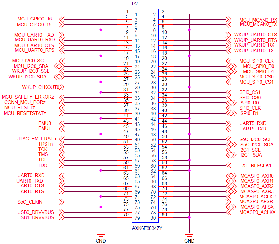
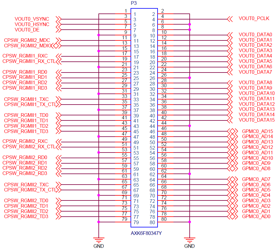
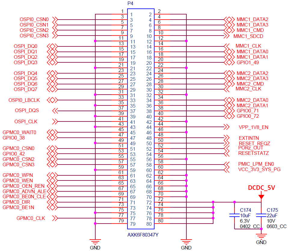
FET62xx-C SoM Pins Schematic are as follows:
2.6.2 FET62xx SoM Pin Functions Description
Note1:
Num ——SoM connector pin no.:
Ball —— CPU pin ball no.
GPIO ——CPU pin general I/O port serial number
Vol ——Pin signal level
Note2:
Signal Name——SoM connector network name, the top right corner subscripts’ meaning are as follows:
Superscript No. |
Superscript Description |
|---|---|
[1] |
Pins can be configured for interrupt use. |
[2] |
The default pin level is 1.8 V. |
[3] |
Pins are CPU boot-related pins, which are not recommended for IO. |
[4] |
Special-purpose pins and can not be used as IO. |
Pin Description—— SoM Pin Signal Descriptions
Default function-All pin functions of the SoM are specified according to the “default function” in the table below. Please do not modify it, otherwise it may be delivered from the factory.
Drive conflict. If you have any questions, please contact our sales or technical support.
Note3: The pins marked as “Do not use on carrier board” in the “Default Function” column are those already utilized by the core board and should not be used in the design of the baseboard.
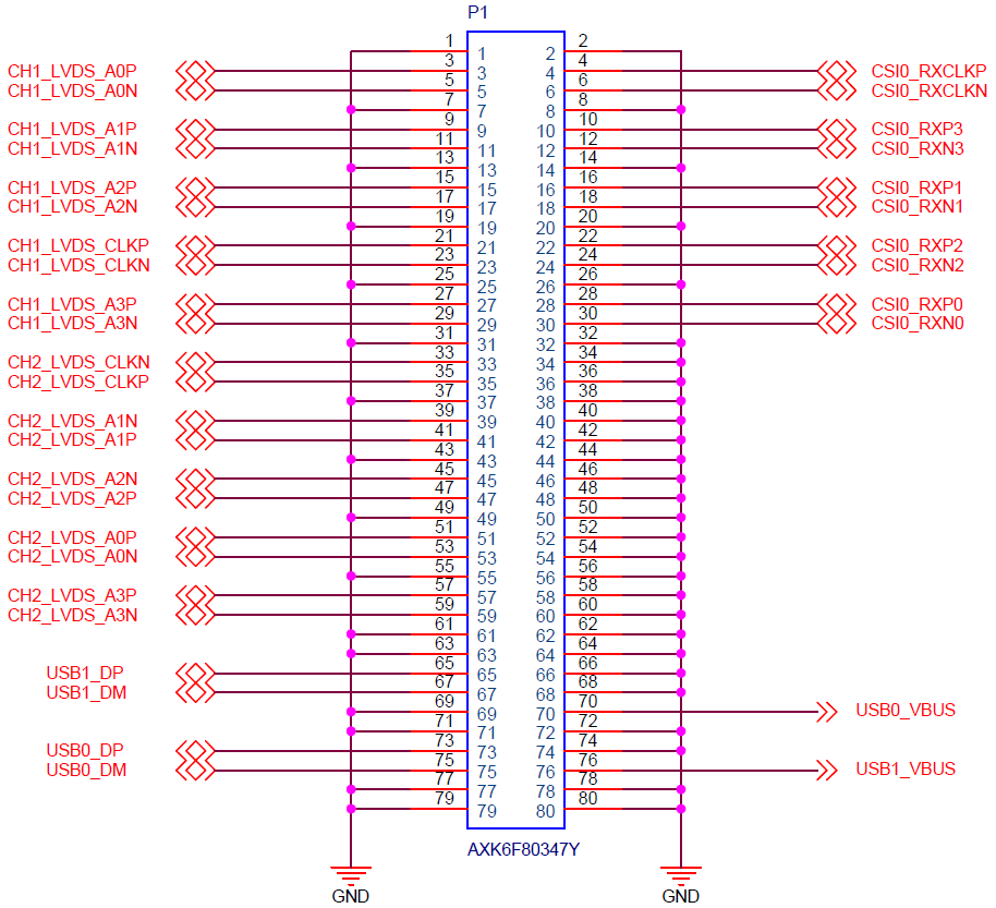
Table 1 LEFT_UP(P1) Connector Interface(Odd) Pin Definition
NUM |
BALL |
Signal Name |
GPIO |
VOL |
Pin Description |
Default Function |
|---|---|---|---|---|---|---|
1 |
- |
GND |
- |
- |
Ground |
GND |
3 |
- |
CH1_LVDS_A0P |
- |
- |
CH1_LVDS data A0+ |
CH1_LVDS_A0P |
5 |
- |
CH1_LVDS_A0N |
- |
- |
CH1_LVDS data A0- |
CH1_LVDS_A0N |
7 |
- |
GND |
- |
- |
Ground |
GND |
9 |
- |
CH1_LVDS_A1P |
- |
- |
CH1_LVDS data A1+ |
CH1_LVDS_A1P |
11 |
- |
CH1_LVDS_A1N |
- |
- |
CH1_LVDS data A1- |
CH1_LVDS_A1N |
13 |
- |
GND |
- |
- |
Ground |
GND |
15 |
- |
CH1_LVDS_A2P |
- |
- |
CH1_LVDS data A2+ |
CH1_LVDS_A2P |
17 |
- |
CH1_LVDS_A2N |
- |
- |
CH1_LVDS data A2- |
CH1_LVDS_A2N |
19 |
- |
GND |
- |
- |
Ground |
GND |
21 |
- |
CH1_LVDS_CLKP |
- |
- |
CH1_LVDS clock+ |
CH1_LVDS_CLKP |
23 |
- |
CH1_LVDS_CLKN |
- |
- |
CH1_LVDS clock- |
CH1_LVDS_CLKN |
25 |
- |
GND |
- |
- |
Ground |
GND |
27 |
- |
CH1_LVDS_A3P |
- |
- |
CH1_LVDS data A3+ |
CH1_LVDS_A3P |
29 |
- |
CH1_LVDS_A3N |
- |
- |
CH1_LVDS data A3- |
CH1_LVDS_A3N |
31 |
- |
GND |
- |
- |
Ground |
GND |
33 |
- |
CH2_LVDS_CLKN |
- |
- |
CH2_LVDS clock- |
CH2_LVDS_CLKN |
35 |
- |
CH2_LVDS_CLKP |
- |
- |
CH2_LVDS clock+ |
CH2_LVDS_CLKP |
37 |
- |
GND |
- |
- |
Ground |
GND |
39 |
- |
CH2_LVDS_A1N |
- |
- |
CH2_LVDS data A1- |
CH2_LVDS_A1N |
41 |
- |
CH2_LVDS_A1P |
- |
- |
CH2_LVDS data A1+ |
CH2_LVDS_A1P |
43 |
- |
GND |
- |
- |
Ground |
GND |
45 |
- |
CH2_LVDS_A2N |
- |
- |
CH2_LVDS data A2- |
CH2_LVDS_A2N |
47 |
- |
CH2_LVDS_A2P |
- |
- |
CH2_LVDS data A2+ |
CH2_LVDS_A2P |
49 |
- |
GND |
- |
- |
Ground |
GND |
51 |
- |
CH2_LVDS_A0P |
- |
- |
CH2_LVDS data A0+ |
CH2_LVDS_A0P |
53 |
- |
CH2_LVDS_A0N |
- |
- |
CH2_LCDS data A0- |
CH2_LVDS_A0N |
55 |
- |
GND |
- |
- |
Ground |
GND |
57 |
- |
CH2_LVDS_A3P |
- |
- |
CH2_LVDS data A3+ |
CH2_LVDS_A3P |
59 |
- |
CH2_LVDS_A3N |
- |
- |
CH2_LVDS data A3- |
CH2_LVDS_A3N |
61 |
- |
GND |
- |
- |
Ground |
GND |
63 |
- |
GND |
- |
- |
Ground |
GND |
65 |
- |
USB1_DP |
- |
- |
USB1 data+ |
USB1_DP |
67 |
- |
USB1_DM |
- |
- |
USB1 data- |
USB1_DM |
69 |
- |
GND |
- |
- |
Ground |
GND |
71 |
- |
GND |
- |
- |
Ground |
GND |
73 |
- |
USB0_DP |
- |
- |
USB0 data+ |
USB0_DP |
75 |
- |
USB0_DM |
- |
- |
USB0 data- |
USB0_DM |
77 |
- |
GND |
- |
- |
Ground |
GND |
79 |
- |
GND |
- |
- |
Ground |
GND |
Table 2 LEFT_UP(P1) Connector Interface(Even) Pin Definition
NUM |
BALL |
Signal Name |
GPIO |
VOL |
Pin Description |
Default Function |
|---|---|---|---|---|---|---|
2 |
- |
GND |
- |
- |
Ground |
GND |
4 |
- |
CSI0_RXCLKP |
- |
- |
MIPI_CSI0 Receiving clock+ |
CSI0_RXCLKP |
6 |
- |
CSI0_RXCLKN |
- |
- |
MIPI_CSI0 Receiving clock- |
CSI0_RXCLKN |
8 |
- |
GND |
- |
- |
Ground |
GND |
10 |
- |
CSI0_RXP3 |
- |
- |
MIPI_CSI0 Receiving data 3+ |
CSI0_RXP3 |
12 |
- |
CSI0_RXN3 |
- |
- |
MIPI_CSI0 Receiving data 3- |
CSI0_RXN3 |
14 |
- |
GND |
- |
- |
Ground |
GND |
16 |
- |
CSI0_RXP1 |
- |
- |
MIPI_CSI0 Receiving data1+ |
CSI0_RXP1 |
18 |
- |
CSI0_RXN1 |
- |
- |
MIPI_CSI0 Receiving data1- |
CSI0_RXN1 |
20 |
- |
GND |
- |
- |
Ground |
GND |
22 |
- |
CSI0_RXP2 |
- |
- |
MIPI_CSI0 Receiving data 2+ |
CSI0_RXP2 |
24 |
- |
CSI0_RXN2 |
- |
- |
MIPI_CSI0 Receiving data 2- |
CSI0_RXN2 |
26 |
- |
GND |
- |
- |
Ground |
GND |
28 |
- |
CSI0_RXP0 |
- |
- |
MIPI_CSI0 Receiving data 0+ |
CSI0_RXP0 |
30 |
- |
CSI0_RXN0 |
- |
- |
MIPI_CSI0 Receiving data 0- |
CSI0_RXN0 |
32 |
- |
GND |
- |
- |
Ground |
GND |
34 |
- |
GND |
- |
- |
Ground |
GND |
36 |
- |
GND |
- |
- |
Ground |
GND |
38 |
- |
GND |
- |
- |
Ground |
GND |
40 |
- |
GND |
- |
- |
Ground |
GND |
42 |
- |
GND |
- |
- |
Ground |
GND |
44 |
- |
GND |
- |
- |
Ground |
GND |
46 |
- |
GND |
- |
- |
Ground |
GND |
48 |
- |
GND |
- |
- |
Ground |
GND |
50 |
- |
GND |
- |
- |
Ground |
GND |
52 |
- |
GND |
- |
- |
Ground |
GND |
54 |
- |
GND |
- |
- |
Ground |
GND |
56 |
- |
GND |
- |
- |
Ground |
GND |
58 |
- |
GND |
- |
- |
Ground |
GND |
60 |
- |
GND |
- |
- |
Ground |
GND |
62 |
- |
GND |
- |
- |
Ground |
GND |
64 |
- |
GND |
- |
- |
Ground |
GND |
66 |
- |
GND |
- |
- |
Ground |
GND |
68 |
- |
GND |
- |
- |
Ground |
GND |
70 |
- |
USB0_VBUS |
- |
1.8V |
USB0_VBUS detection input |
USB0_VBUS |
72 |
- |
GND |
- |
- |
Ground |
GND |
74 |
- |
GND |
- |
- |
Ground |
GND |
76 |
- |
USB1_VBUS |
- |
1.8V |
USB1_VBUS detection input |
USB1_VBUS |
78 |
- |
GND |
- |
- |
Ground |
GND |
80 |
- |
GND |
- |
- |
Ground |
GND |
Table 3 RIGHT_UP(P2) Connector Interface(Odd) Pin Definition
NUM |
BALL |
Signal Name |
GPIO |
VOL |
Pin Description |
Default Function |
|---|---|---|---|---|---|---|
1 |
- |
GND |
- |
- |
Ground |
GND |
3 |
D4 |
MCU_GPIO0_16 |
MCU_GPIO0_16 |
3.3V |
MCU domain GPIO0_16 |
MCU_GPIO0_16 |
5 |
E5 |
MCU_GPIO0_15 |
MCU_GPIO0_16 |
3.3V |
MCU domain GPIO0_15 |
MCU_GPIO0_15 |
7 |
- |
GND |
- |
- |
Ground |
GND |
9 |
A5 |
MCU_UART0_TXD |
MCU_GPIO0_6 |
3.3V |
MCU domain UART0 send |
MCU_UART0_TXD |
11 |
B5 |
MCU_UART0_RXD |
MCU_GPIO0_5 |
3.3V |
MCU domain UART0 receive |
MCU_UART0_RXD |
13 |
A6 |
MCU_UART0_CTS |
MCU_GPIO0_7 |
3.3V |
MCU domain UART0 clear to send (active low) |
MCU_GPIO0_7 |
15 |
B6 |
MCU_UART0_RTS |
MCU_GPIO0_8 |
3.3V |
MCU domain UART0 request to send (active low) |
MCU_GPIO0_8 |
17 |
- |
GND |
- |
- |
Ground |
GND |
19 |
A8 |
MCU_I2C0_SCL |
MCU_GPIO0_17 |
3.3V |
MCU domain I2C0 clock |
MCU_I2C0_SCL |
21 |
D10 |
MCU_I2C0_SDA |
MCU_GPIO0_18 |
3.3V |
MCU domain I2C0 data |
MCU_I2C0_SDA |
23 |
B9 |
WKUP_I2C0_SCL |
MCU_GPIO0_19 |
3.3V |
WKUP domain I2C0 clock |
WKUP_I2C0_SCL |
25 |
A9 |
WKUP_I2C0_SDA |
MCU_GPIO0_20 |
3.3V |
WKUP domain I2C0 data |
WKUP_I2C0_SDA |
27 |
- |
GND |
- |
- |
Ground |
GND |
29 |
A12 |
WKUP_CLKOUT0 |
MCU_GPIO0_23 |
3.3V |
WKUP domain CLKOUT0 output |
WKUP_CLKOUT0 |
31 |
- |
GND |
- |
- |
Ground |
GND |
33 |
- |
MCU_SAFETY_ERRORZ |
- |
1.8V |
MCU domain ESM error signal output |
MCU_SAFETY_ERRORZ |
35 |
- |
CONN_MCU_PORZ |
- |
3.3V |
MCU domain cold reset input |
CONN_MCU_PORZ |
37 |
- |
MCU_RESETZ |
- |
3.3V |
MCU domain warm reset input |
MCU_RESETZ |
39 |
- |
MCU_RESETSTATZ |
- |
3.3V |
MCU domain hot reset status output |
MCU_RESETSTATZ |
41 |
- |
GND |
- |
- |
Ground |
GND |
43 |
- |
EMU0 |
- |
3.3V |
Simulation control 0 |
EMU0 |
45 |
- |
EMU1 |
- |
3.3V |
Simulation control 1 |
EMU1 |
47 |
- |
GND |
- |
- |
Ground |
GND |
49 |
- |
JTAG_EMU_RSTN |
- |
3.3V |
JTAG_EMU cold reset |
JTAG_EMU_RSTN |
51 |
B10 |
TRSTN |
- |
3.3V |
JTAG reset |
TRSTN |
53 |
A10 |
TCK |
- |
3.3V |
JTAG test clock input |
TCK |
55 |
B11 |
TMS |
- |
3.3V |
JTAG test mode selection input |
TMS |
57 |
A11 |
TDI |
- |
3.3V |
JTAG test data input |
TDI |
59 |
D12 |
TDO |
- |
3.3V |
JTAG test data output |
TDO |
61 |
- |
GND |
- |
- |
Ground |
GND |
63 |
D14 |
UART0_RXD |
GPIO1_20 |
3.3V |
Main domain UART0 receive |
UART0_RXD |
65 |
E14 |
UART0_TXD |
GPIO1_21 |
3.3V |
Main domain UART0 send |
UART0_TXD |
67 |
A15 |
UART0_CTS |
GPIO1_22 |
3.3V |
Main domain UART0 clear sending(active low) |
GPIO1_22 |
69 |
B15 |
UART0_RTS |
GPIO1_23 |
3.3V |
Main domain UART0 request to send (active low) |
AUDIO_EXT_REFCLK1 |
71 |
- |
GND |
- |
- |
Ground |
GND |
73 |
- |
SOC_CLKIN |
- |
1.8V |
SoM clock input (floating by default) |
SOC_CLKIN |
75 |
- |
GND |
- |
- |
Ground |
GND |
77 |
- |
USB0_DRVVBUS |
- |
3.3V |
USB0 VBUS control output |
USB0_DRVVBUS |
79 |
- |
USB1_DRVVBUS |
- |
3.3V |
USB1 VBUS control output |
USB1_DRVVBUS |
Table 4 RIGHT_UP(P2) Connector Interface(Even) Pin Definition
NUM |
BALL |
Signal Name |
GPIO |
VOL |
Pin Description |
Default Function |
|---|---|---|---|---|---|---|
2 |
- |
GND |
- |
- |
Ground |
GND |
4 |
B3 |
MCU_MCAN0_RX |
MCU_GPIO0_14 |
3.3V |
MCU domain CAN0 receive |
MCU_MCAN0_RX |
6 |
D6 |
MCU_MCAN0_TX |
MCU_GPIO0_13 |
3.3V |
MCU domain CAN0 send |
MCU_MCAN0_TX |
8 |
- |
GND |
- |
- |
Ground |
GND |
10 |
C6 |
WKUP_UART0_CTS |
MCU_GPIO0_11 |
3.3V |
WKUP domain UART0 clear sending |
MCU_GPIO0_11 |
12 |
A4 |
WKUP_UART0_RTS |
MCU_GPIO0_12 |
3.3V |
WKUP domain UART0 request to send |
MCU_GPIO0_12 |
14 |
B4 |
WKUP_UART0_RX |
MCU_GPIO0_9 |
3.3V |
WKUP domain UART0 receive |
WKUP_UART0_RX |
16 |
C5 |
WKUP_UART0_TX |
MCU_GPIO0_10 |
3.3V |
WKUP domain UART0 send |
WKUP_UART0_TX |
18 |
- |
GND |
- |
- |
Ground |
GND |
20 |
A7 |
MCU_SPI0_CLK |
MCU_GPIO0_2 |
3.3V |
MCU domain SPI0 clock |
MCU_SPI0_CLK |
22 |
D9 |
MCU_SPI0_D0 |
MCU_GPIO0_3 |
3.3V |
MCU domain SPI0 data 0 |
MCU_SPI0_D0 |
24 |
C9 |
MCU_SPI0_D1 |
MCU_GPIO0_4 |
3.3V |
MCU domain SPI0 data 1 |
MCU_SPI0_D1 |
26 |
E8 |
MCU_SPI0_CS0 |
MCU_GPIO0_0 |
3.3V |
MCU domain SPI0 chip selection 0 |
MCU_SPI0_CS0 |
28 |
B8 |
MCU_SPI0_CS1 |
MCU_GPIO0_1 |
3.3V |
MCU domain SPI0 chip selection 1 |
MCU_SPI0_CS1 |
30 |
- |
GND |
- |
- |
Ground |
GND |
32 |
C13 |
SPI0_CS1 |
GPIO1_16 |
3.3V |
Main domain SPI0 chip selection 1 |
GPIO1_16 |
34 |
A13 |
SPI0_CS0 |
GPIO1_15 |
3.3V |
Main domain SPI0 chip selection 0 |
GPIO1_15 |
36 |
B13 |
SPI0_D0 |
GPIO1_18 |
3.3V |
Main domain SPI0 data 0 |
GPIO1_18 |
38 |
A14 |
SPI0_CLK |
GPIO1_17 |
3.3V |
Main domain SPI0 clock |
GPIO1_17 |
40 |
B14 |
SPI0_D1 |
GPIO1_19 |
3.3V |
Main domain SPI0 data 1 |
GPIO1_19 |
42 |
- |
GND |
- |
- |
Ground |
GND |
44 |
C15 |
UART5_RXD |
GPIO1_24 |
3.3V |
Main domain UART5 receive |
UART5_RXD |
46 |
E15 |
UART5_TXD |
GPIO1_25 |
3.3V |
Main domain UART5 send |
UART5_TXD |
48 |
- |
GND |
- |
- |
Ground |
GND |
50 |
B16 |
SOC_I2C0_SCL |
GPIO1_26 |
3.3V |
Main domain I2C0 clock |
SOC_I2C0_SCL |
52 |
A16 |
SOC_I2C0_SDA |
GPIO1_27 |
3.3V |
Main domain I2C0 data |
SOC_I2C0_SDA |
54 |
B17 |
I2C1_SCL |
GPIO1_28 |
3.3V |
Main domain I2C1 clock |
I2C1_SCL |
56 |
A17 |
I2C1_SDA |
GPIO1_29 |
3.3V |
Main domain I2C1 data |
I2C1_SDA |
58 |
- |
GND |
- |
- |
Ground |
GND |
60 |
- |
EXT_REFCLK1 |
- |
3.3V |
External clock input to the Main domain |
EXT_REFCLK1 |
62 |
- |
GND |
- |
- |
Ground |
GND |
64 |
E18 |
MCASP0_AXR0 |
GPIO1_10 |
3.3V |
MCASP0 serial data 0 |
LCD_PWM |
66 |
B18 |
MCASP0_AXR1 |
GPIO1_9 |
3.3V |
MCASP0 serial data 1 |
LVDS_PWM |
68 |
A19 |
MCASP0_AXR2 |
GPIO1_8 |
3.3V |
MCASP0 serial data 2 |
MCASP0_AXR2 |
70 |
B19 |
MCASP0_AXR3 |
GPIO1_7 |
3.3V |
MCASP0 serial data 3 |
MCASP0_AXR3 |
72 |
A20 |
MCASP0_ACLKR |
GPIO1_14 |
3.3V |
MCASP0 receive bit reference clock |
MCASP0_ACLKR |
74 |
E19 |
MCASP0_AFSR |
GPIO1_13 |
3.3V |
MCASP0 receives the frame sync |
MCASP0_AFSR |
76 |
D20 |
MCASP0_AFSX |
GPIO1_12 |
3.3V |
MCASP0 send bit reference clock |
MCASP0_AFSX |
78 |
B20 |
MCASP0_ACLKX |
GPIO1_11 |
3.3V |
MCASP0 sends frame sync |
MCASP0_ACLKX |
80 |
- |
GND |
- |
- |
Ground |
GND |
Table 5 LEFT _ DOWN (P3) Connector Interface (Odd) Pin Definition
NUM |
BALL |
Signal Name |
GPIO |
VOL |
Pin Description |
Default Function |
|---|---|---|---|---|---|---|
1 |
- |
GND |
- |
- |
Ground |
GND |
3 |
AC25 |
VOUT0_VSYNC |
GPIO0_63 |
3.3V |
Vertical synchronization of video output |
VOUT0_VSYNC |
5 |
AB24 |
VOUT0_HSYNC |
GPIO0_61 |
3.3V |
Horizontal synchronization of video output |
VOUT0_HSYNC |
7 |
Y20 |
VOUT0_DE |
GPIO0_62 |
3.3V |
Enable video output data |
VOUT0_DE |
9 |
- |
GND |
- |
- |
Ground |
GND |
11 |
AD24 |
CPSW_RGMII2_MDC |
GPIO0_86 |
3.3V |
MDIO clock |
CPSW_RGMII2_MDC |
13 |
AB22 |
CPSW_RGMII2_MDIO |
GPIO0_85 |
3.3V |
MDIO data |
CPSW_RGMII2_MDIO |
15 |
- |
GND |
- |
- |
Ground |
GND |
17 |
AD17 |
CPSW_RGMII1_RXC |
GPIO0_80 |
3.3V |
RGMII1 Receiving clock- |
CPSW_RGMII1_RXC |
19 |
AE17 |
CPSW_RGMII1_RX_CTL |
GPIO0_79 |
3.3V |
RGMII1 receiving control |
CPSW_RGMII1_RX_CTL |
21 |
- |
GND |
- |
- |
Ground |
GND |
23 |
AB17 |
CPSW_RGMII1_RD0 |
GPIO0_81 |
3.3V |
RGMII1 receive data 0 |
CPSW_RGMII1_RD0 |
25 |
AC17 |
CPSW_RGMII1_RD1 |
GPIO0_82 |
3.3V |
RGMII1 receive data 1 |
CPSW_RGMII1_RD1 |
27 |
AB16 |
CPSW_RGMII1_RD2 |
GPIO0_83 |
3.3V |
RGMII1 receive data 2 |
CPSW_RGMII1_RD2 |
29 |
AA15 |
CPSW_RGMII1_RD3 |
GPIO0_84 |
3.3V |
RGMII1 receive data 3 |
CPSW_RGMII1_RD3 |
31 |
- |
GND |
- |
- |
Ground |
GND |
33 |
AE19 |
CPSW_RGMII1_TXC |
GPIO0_74 |
3.3V |
RGMII1 clock sending |
CPSW_RGMII1_TXC |
35 |
AD19 |
CPSW_RGMII1_TX_CTL |
GPIO0_73 |
3.3V |
RGMII1 sending control |
CPSW_RGMII1_TX_CTL |
37 |
- |
GND |
- |
- |
Ground |
GND |
39 |
AE20 |
CPSW_RGMII1_TD0 |
GPIO0_75 |
3.3V |
RGMII1 sends data 0 |
CPSW_RGMII1_TD0 |
41 |
AD20 |
CPSW_RGMII1_TD1 |
GPIO0_76 |
3.3V |
RGMII1 sends data 1 |
CPSW_RGMII1_TD1 |
43 |
AE18 |
CPSW_RGMII1_TD2 |
GPIO0_77 |
3.3V |
RGMII1 sends data 2 |
CPSW_RGMII1_TD2 |
45 |
AD18 |
CPSW_RGMII1_TD3 |
GPIO0_78 |
3.3V |
RGMII1_send data 3 |
CPSW_RGMII1_TD3 |
47 |
- |
GND |
- |
- |
Ground |
GND |
49 |
AD23 |
CPSW_RGMII2_RXC |
GPIO1_2 |
3.3V |
RGMII2 Receiving clock- |
CPSW_RGMII2_RXC |
51 |
AD22 |
CPSW_RGMII2_RX_CTL |
GPIO1_1 |
3.3V |
RGMII2 receiving control |
CPSW_RGMII2_RX_CTL |
53 |
- |
GND |
- |
- |
Ground |
GND |
55 |
AE23 |
CPSW_RGMII2_RD0 |
GPIO1_3 |
3.3V |
RGMII2 receive data 0 |
CPSW_RGMII2_RD0 |
57 |
AB20 |
CPSW_RGMII2_RD1 |
GPIO1_4 |
3.3V |
RGMII2 receive data 1 |
CPSW_RGMII2_RD1 |
59 |
AC21 |
CPSW_RGMII2_RD2 |
GPIO1_5 |
3.3V |
RGMII2 receive data 2 |
CPSW_RGMII2_RD2 |
61 |
AE22 |
CPSW_RGMII2_RD3 |
GPIO1_6 |
3.3V |
RGMII2 receive data 3 |
CPSW_RGMII2_RD3 |
63 |
- |
GND |
- |
- |
Ground |
GND |
65 |
AE21 |
CPSW_RGMII2_TXC |
GPIO0_88 |
3.3V |
RGMII2 clock sending |
CPSW_RGMII2_TXC |
67 |
AA19 |
CPSW_RGMII2_TX_CTL |
GPIO0_87 |
3.3V |
RGMII2 sending control |
CPSW_RGMII2_TX_CTL |
69 |
- |
GND |
- |
- |
Ground |
GND |
71 |
Y18 |
CPSW_RGMII2_TD0 |
GPIO0_89 |
3.3V |
RGMII2 sends data 0 |
CPSW_RGMII2_TD0 |
73 |
AA18 |
CPSW_RGMII2_TD1 |
GPIO0_90 |
3.3V |
RGMII2 sends data 1 |
CPSW_RGMII2_TD1 |
75 |
AD21 |
CPSW_RGMII2_TD2 |
GPIO0_91 |
3.3V |
RGMII2 sends data 2 |
CPSW_RGMII2_TD2 |
77 |
AC20 |
CPSW_RGMII2_TD3 |
GPIO1_0 |
3.3V |
RGMII2 sends data 3 |
CPSW_RGMII2_TD3 |
79 |
- |
GND |
- |
- |
Ground |
GND |
Table 6 LEFT _ DOWN (P3) Connector Interface (Even) Pin Definition
NUM |
BALL |
Signal Name |
GPIO |
VOL |
Pin Description |
Default Function |
|---|---|---|---|---|---|---|
2 |
- |
GND |
- |
- |
Ground |
GND |
4 |
AC24 |
VOUT0_PCLK |
GPIO0_64 |
3.3V |
Video output pixel clock |
VOUT0_PCLK |
6 |
- |
GND |
- |
- |
Ground |
GND |
8 |
- |
GND |
- |
- |
Ground |
GND |
10 |
U22 |
VOUT0_DATA0 |
GPIO0_45 |
3.3V |
Video output data 0 |
VOUT0_DATA0 |
12 |
V24 |
VOUT0_DATA1 |
GPIO0_46 |
3.3V |
Video output data 1 |
VOUT0_DATA1 |
14 |
W25 |
VOUT0_DATA2 |
GPIO0_47 |
3.3V |
Video output data 2 |
VOUT0_DATA2 |
16 |
W24 |
VOUT0_DATA3 |
GPIO0_48 |
3.3V |
Video output data 3 |
VOUT0_DATA3 |
18 |
Y25 |
VOUT0_DATA4 |
GPIO0_49 |
3.3V |
Video output data 4 |
VOUT0_DATA4 |
20 |
Y24 |
VOUT0_DATA5 |
GPIO0_50 |
3.3V |
Video output data 5 |
VOUT0_DATA5 |
22 |
Y23 |
VOUT0_DATA6 |
GPIO0_51 |
3.3V |
Video output data 6 |
VOUT0_DATA6 |
24 |
AA25 |
VOUT0_DATA7 |
GPIO0_52 |
3.3V |
Video output data 7 |
VOUT0_DATA7 |
26 |
- |
GND |
- |
- |
Ground |
GND |
28 |
V21 |
VOUT0_DATA8 |
GPIO0_53 |
3.3V |
Video output data 8 |
VOUT0_DATA8 |
30 |
W21 |
VOUT0_DATA9 |
GPIO0_54 |
3.3V |
Video output data 9 |
VOUT0_DATA9 |
32 |
V20 |
VOUT0_DATA10 |
GPIO0_55 |
3.3V |
Video output data 10 |
VOUT0_DATA10 |
34 |
AA23 |
VOUT0_DATA11 |
GPIO0_56 |
3.3V |
Video output data 11 |
VOUT0_DATA11 |
36 |
AB25 |
VOUT0_DATA12 |
GPIO0_57 |
3.3V |
Video output data 12 |
VOUT0_DATA12 |
38 |
AA24 |
VOUT0_DATA13 |
GPIO0_58 |
3.3V |
Video output data 13 |
VOUT0_DATA13 |
40 |
Y22 |
VOUT0_DATA14 |
GPIO0_59 |
3.3V |
Video output data 14 |
VOUT0_DATA14 |
42 |
AA21 |
VOUT0_DATA15 |
GPIO0_60 |
3.3V |
Video output data 15 |
VOUT0_DATA15 |
44 |
- |
GND |
- |
- |
Ground |
GND |
46 |
U24 |
GPMC0_AD15 |
GPIO0_30 |
3.3V |
GPMC data 15/address 16 |
GPMC0_AD15 |
48 |
U25 |
GPMC0_AD14 |
GPIO0_29 |
3.3V |
GPMC data 14/address 15 |
GPMC0_AD14 |
50 |
T24 |
GPMC0_AD13 |
GPIO0_28 |
3.3V |
GPMC data 13/address 14 |
GPMC0_AD13 |
52 |
T22 |
GPMC0_AD12 |
GPIO0_27 |
3.3V |
GPMC data 12/address 13 |
GPMC0_AD12 |
54 |
R21 |
GPMC0_AD11 |
GPIO0_26 |
3.3V |
GPMC data 11/address 12 |
GPMC0_AD11 |
56 |
T25 |
GPMC0_AD10 |
GPIO0_25 |
3.3V |
GPMC data 10/address 11 |
GPMC0_AD10 |
58 |
R25 |
GPMC0_AD9 |
GPIO0_24 |
3.3V |
GPMC data 9/address 10 |
GPMC0_AD9 |
60 |
R24 |
GPMC0_AD8 |
GPIO0_23 |
3.3V |
GPMC data 8/address 9 |
GPMC0_AD8 |
62 |
- |
GND |
- |
- |
Ground |
GND |
64 |
R23 |
GPMC0_AD7 |
GPIO0_22 |
3.3V |
GPMC data 7/address 8 |
GPMC0_AD7 |
66 |
P21 |
GPMC0_AD6 |
GPIO0_21 |
3.3V |
GPMC data 6/address 7 |
GPMC0_AD6 |
68 |
P22 |
GPMC0_AD5 |
GPIO0_20 |
3.3V |
GPMC data 5/address 6 |
GPMC0_AD5 |
70 |
P24 |
GPMC0_AD4 |
GPIO0_19 |
3.3V |
GPMC data 4/address 5 |
GPMC0_AD4 |
72 |
N25 |
GPMC0_AD3 |
GPIO0_18 |
3.3V |
GPMC data 3/address 4 |
GPMC0_AD3 |
74 |
N24 |
GPMC0_AD2 |
GPIO0_17 |
3.3V |
GPMC data 2/address 3 |
GPMC0_AD2 |
76 |
N23 |
GPMC0_AD1 |
GPIO0_16 |
3.3V |
GPMC data 1/address 2 |
GPMC0_AD1 |
78 |
M25 |
GPMC0_AD0 |
GPIO0_15 |
3.3V |
GPMC data 0/address 1 |
GPMC0_AD0 |
80 |
- |
GND |
- |
- |
Ground |
GND |
Table 7. RIGHT_ DOWN (P4) Connector Interface (Odd) Pin Definition
NUM |
BALL |
Signal Name |
GPIO |
VOL |
Pin Description |
Default Function |
|---|---|---|---|---|---|---|
1 |
- |
GND |
- |
- |
Ground |
GND |
3 |
F23 |
OSPI0_CSN0 |
GPIO0_11 |
1.8V |
OSPI chip select 0 |
OSPI0_CSN0 |
5 |
G21 |
OSPI0_CSN1 |
GPIO0_12 |
1.8V |
OSPI chip select 1 |
GPIO0_12 |
7 |
H21 |
OSPI0_CSN2 |
GPIO0_13 |
1.8V |
OSPI chip select 2 |
OSPI0_CSN2 |
9 |
E24 |
OSPI0_CSN3 |
GPIO0_14 |
1.8V |
OSPI chip select 3 |
OSPI0_CSN3 |
11 |
- |
GND |
- |
- |
Ground |
GND |
13 |
E25 |
OSPI_DQ0 |
GPIO0_3 |
1.8V |
OSPI Data 0 |
OSPI_DQ0 |
15 |
G24 |
OSPI_DQ1 |
GPIO0_4 |
1.8V |
OSPI Data 1 |
OSPI_DQ1 |
17 |
F25 |
OSPI_DQ2 |
GPIO0_5 |
1.8V |
OSPI Data 2 |
OSPI_DQ2 |
19 |
F24 |
OSPI_DQ3 |
GPIO0_6 |
1.8V |
OSPI Data 3 |
OSPI_DQ3 |
21 |
- |
GND |
- |
- |
Ground |
GND |
23 |
J23 |
OSPI_DQ4 |
GPIO0_7 |
1.8V |
OSPI Data 4 |
GPIO0_7 |
25 |
J25 |
OSPI_DQ5 |
GPIO0_8 |
1.8V |
OSPI Data 5 |
GPIO0_8 |
27 |
H25 |
OSPI_DQ6 |
GPIO0_9 |
1.8V |
OSPI Data 6 |
GPIO0_9 |
29 |
J22 |
OSPI_DQ7 |
GPIO0_10 |
1.8V |
OSPI Data 7 |
GPIO0_10 |
31 |
- |
GND |
- |
- |
Ground |
GND |
33 |
G25 |
OSPI0_LBCLK |
GPIO0_1 |
1.8V |
OSPI loop clock input/output |
OSPI0_LBCLK |
35 |
- |
GND |
- |
- |
Ground |
GND |
37 |
J24 |
OSPI_DQS |
GPIO0_2 |
1.8V |
OSPI data strobe or loopback clock input |
OSPI_DQS |
39 |
- |
GND |
- |
- |
Ground |
GND |
41 |
H24 |
OSPI_CLK |
GPIO0_0 |
1.8V |
OSPI clock output- |
OSPI_CLK |
43 |
- |
GND |
- |
- |
Ground |
GND |
45 |
U23 |
GPMC0_WAIT0 |
GPIO0_37 |
3.3V |
GPMC external wait for indication input |
GPMC0_WAIT0 |
47 |
V25 |
GPIO0_38 |
GPIO0_38 |
3.3V |
Main domain GPIO0_38 |
GPIO0_38 |
49 |
- |
GND |
- |
- |
Ground |
GND |
51 |
M21 |
GPMC0_CSN0 |
GPIO0_41 |
3.3V |
GPMC chip select 0 |
GPMC0_CSN0 |
53 |
L21 |
GPIO0_42 |
GPIO0_42 |
3.3V |
Main domain GPIO0_42 |
GPIO0_42 |
55 |
K22 |
GPMC0_CSN2 |
GPIO0_43 |
3.3V |
GPMC chip select 2 |
GPMC0_CSN2 |
57 |
K24 |
GPMC0_CSN3 |
GPIO0_44 |
3.3V |
GPMC chip select 3 |
GPMC0_CSN3 |
59 |
- |
GND |
- |
- |
Ground |
GND |
61 |
K25 |
GPMC0_WPN |
GPIO0_39 |
3.3V |
GPMC Flash write protect |
GPIO0_39 |
63 |
L25 |
GPMC0_WEN |
GPIO0_34 |
3.3V |
GPMC write enable |
GPMC0_WEN |
65 |
L24 |
GPMC0_OEN_REN |
GPIO0_33 |
3.3V |
GPMC output enable or read enable |
GPMC0_OEN_REN |
67 |
L23 |
GPMC0_ADVN_ALE |
GPIO0_32 |
3.3V |
GPMC address active (active low) or address latch enable |
GPMC0_ADVN_ALE |
69 |
M24 |
GPMC0_BE0N_CLE |
GPIO0_35 |
3.3V |
GPMC low byte enable or command latch enable |
GPIO0_35 |
71 |
M22 |
GPMC0_DIR |
GPIO0_35 |
3.3V |
GPMC data bus signal direction control |
GPIO0_40 |
73 |
N20 |
GPMC0_BE1N |
GPIO0_36 |
3.3V |
GPMC high byte enable |
GPIO0_36 |
75 |
- |
GND |
- |
- |
Ground |
GND |
77 |
P25 |
GPMC0_CLK |
GPIO0_31 |
3.3V |
GPMC clock output- |
GPIO0_31 |
79 |
- |
GND |
- |
- |
Ground |
GND |
Table 8. RIGHT_ DOWN (P4) Connector Interface (Even) Pin Definition
NUM** |
BALL |
Signal Name |
GPIO |
VOL |
Pin Description |
Default Function |
|---|---|---|---|---|---|---|
2 |
- |
GND |
- |
- |
Ground |
GND |
4 |
C21 |
MMC1_DATA2 |
GPIO1_43 |
1.8V/3.3V |
MMC1 data bit 2- |
MMC1_DATA2 |
6 |
D22 |
MMC1_DATA3 |
GPIO1_42 |
1.8V/3.3V |
MMC1 data bit 3- |
MMC1_DATA3 |
8 |
A21 |
MMC1_CMD |
GPIO1_47 |
1.8V/3.3V |
MMC1 command |
MMC1_CMD |
10 |
D17 |
MMC1_SDCD |
GPIO1_48 |
3.3V |
MMC1 card detection |
MMC1_SDCD |
12 |
- |
GND |
- |
- |
Ground |
GND |
14 |
B22 |
MMC1_CLK |
GPIO1_46 |
1.8V/3.3V |
MMC1 clock |
MMC1_CLK |
16 |
A22 |
MMC1_DATA0 |
GPIO1_45 |
1.8V/3.3V |
MMC1 data bit 0- |
MMC1_DATA0 |
18 |
B21 |
MMC1_DATA1 |
GPIO1_44 |
1.8V/3.3V |
MMC1 data bit 1- |
MMC1_DATA1 |
20 |
C17 |
GPIO1_49 |
GPIO1_49 |
3.3V |
Main domain GPIO1_49 |
GPIO1_49 |
22 |
- |
GND |
- |
- |
Ground |
GND |
24 |
E23 |
MMC2_DATA2 |
GPIO0_66 |
1.8V |
MMC2 data bit 2- |
MMC2_DATA2 |
26 |
D24 |
MMC2_DATA3 |
GPIO0_65 |
1.8V |
MMC2 data bit 3- |
MMC2_DATA3 |
28 |
C24 |
MMC2_CMD |
GPIO0_70 |
1.8V |
MMC2 command |
MMC2_CMD |
30 |
D25 |
MMC2_CLK |
GPIO0_69 |
1.8V |
MMC2 clock |
MMC2_CLK |
32 |
- |
GND |
- |
- |
Ground |
GND |
34 |
B24 |
MMC2_DATA0 |
GPIO0_68 |
1.8V |
MMC2 data bit 0- |
MMC2_DATA0 |
36 |
C25 |
MMC2_DATA1 |
GPIO0_67 |
1.8V |
MMC2 data bit 1- |
MMC2_DATA1 |
38 |
A23 |
GPIO0_71 |
GPIO0_71 |
1.8V |
Main domain GPIO0_71 |
GPIO0_71 |
40 |
B23 |
GPIO0_72 |
GPIO0_72 |
1.8V |
Main domain GPIO0_72 |
GPIO0_72 |
42 |
- |
GND |
- |
- |
Ground |
GND |
44 |
- |
VPP_1V8_EN |
- |
3.3V |
SoM VPP_1V8 enable input |
VPP_1V8_EN |
46 |
- |
GND |
- |
- |
Ground |
GND |
48 |
- |
EXTINTN |
- |
3.3V |
External interrupt input |
EXTINTN |
50 |
- |
RESET_REQZ |
- |
3.3V |
Main domain external hot reset request input |
RESET_REQZ |
52 |
- |
PORZ_OUT |
- |
3.3V |
Main domain POR status output |
PORZ_OUT |
54 |
- |
RESETSTATZ |
- |
3.3V |
Main domain hot reset state output |
RESETSTATZ |
56 |
- |
GND |
- |
- |
Ground |
GND |
58 |
- |
PMIC_LPM_EN0 |
- |
3.3V |
Dual function PMIC control output, |
PMIC_LPM_EN0 |
60 |
- |
VCC_3V3_SYS_PG |
- |
3.3V |
SoM VCC3V3 Power Good output, |
VCC_3V3_SYS_PG |
62 |
- |
GND |
- |
- |
Ground |
GND |
64 |
- |
GND |
- |
- |
Ground |
GND |
66 |
- |
GND |
- |
- |
Ground |
GND |
68 |
- |
GND |
- |
- |
Ground |
GND |
70 |
- |
GND |
- |
- |
Ground |
GND |
72 |
- |
DCDC_5V |
- |
5V |
SoM 5V power input |
DCDC_5V |
74 |
- |
DCDC_5V |
- |
5V |
SoM 5V power input |
DCDC_5V |
76 |
- |
DCDC_5V |
- |
5V |
SoM 5V power input |
DCDC_5V |
78 |
- |
DCDC_5V |
- |
5V |
SoM 5V power input |
DCDC_5V |
80 |
- |
DCDC_5V |
- |
5V |
SoM 5V power input |
DCDC_5V |
2.7 FET62xx SoM Pin Description (Divided by Function)
Note:
All the pin functions of the SoM are specified according to the “Default Functions” in the following table, please do not modify them, otherwise, they may conflict with the factory driver. Please contact us with any questions in time;
When you have requirements for multiple function expansions, please refer to the “FET62xx-C Pin Multiplexing Comparison Table” in the reference materials. However, if you need more detailed information, please consult relevant documentation, the chip data sheet, and the reference manual;
The pins marked as “Do not use on carrier board” in the “Default Function” column are those already utilized by the SoM and should not be used in the design of the carrier board;
“Signal Name” column defaults to SoM pin name, and the red mark is carrier board pin definition name.
2.7.1 Power Pin
Function |
Signal Name |
I/O |
Default Function |
Pin Number |
|---|---|---|---|---|
Power |
DCDC_5V |
Power Input |
External power supply pin, 5V |
P4_72 |
DCDC_5V |
Power Input |
External power supply pin, 5V |
||
DCDC_5V |
Power Input |
External power supply pin, 5V |
||
DCDC_5V |
Power Input |
External power supply pin, 5V |
||
DCDC_5V |
Power Input |
External power supply pin, 5V |
||
GND |
— |
Power ground |
P1_1 |
|
GND |
— |
Power ground |
P1_2 |
|
GND |
— |
Power ground |
P1_7 |
|
GND |
— |
Power ground |
P1_8 |
|
GND |
— |
Power ground |
P1_13 |
|
GND |
— |
Power ground |
P1_14 |
|
GND |
— |
Power ground |
P1_19 |
|
GND |
— |
Power ground |
P1_20 |
|
GND |
— |
Power ground |
P1_25 |
|
GND |
— |
Power ground |
P1_26 |
|
GND |
— |
Power ground |
P1_31 |
|
GND |
— |
Power ground |
P1_32 |
|
GND |
— |
Power ground |
P1_34 |
|
GND |
— |
Power ground |
P1_36 |
|
GND |
— |
Power ground |
P1_37 |
|
GND |
— |
Power ground |
P1_38 |
|
GND |
— |
Power ground |
P1_40 |
|
GND |
— |
Power ground |
P1_42 |
|
GND |
— |
Power ground |
P1_43 |
|
GND |
— |
Power ground |
P1_44 |
|
GND |
— |
Power ground |
P1_46 |
|
GND |
— |
Power ground |
P1_48 |
|
GND |
— |
Power ground |
P1_49 |
|
GND |
— |
Power ground |
P1_50 |
|
GND |
— |
Power ground |
P1_52 |
|
GND |
— |
Power ground |
P1_54 |
|
GND |
— |
Power ground |
P1_55 |
|
GND |
— |
Power ground |
P1_56 |
|
GND |
— |
Power ground |
P1_58 |
|
GND |
— |
Power ground |
P1_60 |
|
GND |
— |
Power ground |
P1_61 |
|
GND |
— |
Power ground |
P1_62 |
|
GND |
— |
Power ground |
P1_63 |
|
GND |
— |
Power ground |
P1_64 |
|
GND |
— |
Power ground |
P1_66 |
|
GND |
— |
Power ground |
P1_68 |
|
GND |
— |
Power ground |
P1_69 |
|
GND |
— |
Power ground |
P1_71 |
|
GND |
— |
Power ground |
P1_72 |
|
GND |
— |
Power ground |
P1_74 |
|
GND |
— |
Power ground |
P1_77 |
|
GND |
— |
Power ground |
P1_78 |
|
GND |
— |
Power ground |
P1_79 |
|
GND |
— |
Power ground |
P1_80 |
|
GND |
— |
Power ground |
P2_1 |
|
GND |
— |
Power ground |
P2_2 |
|
GND |
— |
Power ground |
P2_7 |
|
GND |
— |
Power ground |
P2_8 |
|
GND |
— |
Power ground |
P2_17 |
|
GND |
— |
Power ground |
P2_18 |
|
GND |
— |
Power ground |
P2_27 |
|
GND |
— |
Power ground |
P2_30 |
|
GND |
— |
Power ground |
P2_31 |
|
GND |
— |
Power ground |
P2_41 |
|
GND |
— |
Power ground |
P2_42 |
|
GND |
— |
Power ground |
P2_47 |
|
GND |
— |
Power ground |
P2_48 |
|
GND |
— |
Power ground |
P2_61 |
|
GND |
— |
Power ground |
P2_62 |
|
GND |
— |
Power ground |
P2_71 |
|
GND |
— |
Power ground |
P2_75 |
|
GND |
— |
Power ground |
P2_80 |
|
GND |
— |
Power ground |
P2_79 |
|
GND |
— |
Power ground |
P2_80 |
|
GND |
— |
Power ground |
P3_1 |
|
GND |
— |
Power ground |
P3_2 |
|
GND |
— |
Power ground |
P3_6 |
|
GND |
— |
Power ground |
P3_8 |
|
GND |
— |
Power ground |
P3_9 |
|
GND |
— |
Power ground |
P3_15 |
|
GND |
— |
Power ground |
P3_21 |
|
GND |
— |
Power ground |
P3_26 |
|
GND |
— |
Power ground |
P3_31 |
|
GND |
— |
Power ground |
P3_37 |
|
GND |
— |
Power ground |
P3_44 |
|
GND |
— |
Power ground |
P3_47 |
|
GND |
— |
Power ground |
P3_53 |
|
GND |
— |
Power ground |
P3_62 |
|
GND |
— |
Power ground |
P3_63 |
|
GND |
— |
Power ground |
P3_69 |
|
GND |
— |
Power ground |
P3_79 |
|
GND |
— |
Power ground |
P3_80 |
|
GND |
— |
Power ground |
P4_1 |
|
GND |
— |
Power ground |
P4_2 |
|
GND |
— |
Power ground |
P4_11 |
|
GND |
— |
Power ground |
P4_12 |
|
GND |
— |
Power ground |
P4_21 |
|
GND |
— |
Power ground |
P4_22 |
|
GND |
— |
Power ground |
P4_31 |
|
GND |
— |
Power ground |
P4_32 |
|
GND |
— |
Power ground |
P4_35 |
|
GND |
— |
Power ground |
P4_39 |
|
GND |
— |
Power ground |
P4_42 |
|
GND |
— |
Power ground |
P4_43 |
|
GND |
— |
Power ground |
P4_46 |
|
GND |
— |
Power ground |
P4_49 |
|
GND |
— |
Power ground |
P4_56 |
|
GND |
— |
Power ground |
P4_59 |
|
GND |
— |
Power ground |
P4_62 |
|
GND |
— |
Power ground |
P4_64 |
|
GND |
— |
Power ground |
P4_66 |
|
GND |
— |
Power ground |
P4_68 |
|
GND |
— |
Power ground |
P4_70 |
|
GND |
— |
Power ground |
P4_75 |
|
GND |
— |
Power ground |
P4_79 |
2.7.2 Boot Control Pin
Note: Refer to “3.5.4 Boot Configuration” for boot startup configuration pin.
Function |
Signal Name |
I/O |
Default Function |
Pin Number |
|---|---|---|---|---|
BOOTMODE |
BOOTMODE00 |
I |
BOOT Mode Configuration 0 |
P3_78 |
BOOTMODE01 |
I |
BOOT Mode Configuration 1 |
P3_76 |
|
BOOTMODE02 |
I |
BOOT Mode Configuration 2 |
P3_74 |
|
BOOTMODE03 |
I |
BOOT Mode Configuration 3 |
P3_72 |
|
BOOTMODE04 |
I |
BOOT Mode Configuration 4 |
P3_70 |
|
BOOTMODE05 |
I |
BOOT Mode Configuration 5 |
P3_68 |
|
BOOTMODE06 |
I |
BOOT Mode Configuration 6 |
P3_66 |
|
BOOTMODE07 |
I |
BOOT Mode Configuration 7 |
P3_64 |
|
BOOTMODE08 |
I |
BOOT Mode Configuration 8 |
P3_60 |
|
BOOTMODE09 |
I |
BOOT Mode Configuration 9 |
P3_58 |
|
BOOTMODE10 |
I |
BOOT Mode Configuration 10 |
P3_56 |
|
BOOTMODE11 |
I |
BOOT Mode Configuration 11 |
P3_54 |
|
BOOTMODE12 |
I |
BOOT Mode Configuration 12 |
P3_52 |
|
BOOTMODE13 |
I |
BOOT Mode Configuration 13 |
P3_50 |
|
BOOTMODE14 |
I |
BOOT Mode Configuration 14 |
P3_48 |
|
BOOTMODE15 |
I |
BOOT Mode Configuration 15 |
P3_46 |
2.7.3 LVDS Output Pin
MAIN Domain:
Function |
Signal Name |
I/O |
Default Function |
Pin Number |
|---|---|---|---|---|
LVDS |
CH1_LVDS_A0P |
O |
CH1_LVDS data 0+ |
P1_3 |
CH1_LVDS_A0N |
O |
CH1_LVDS data bit 0- |
P1_5 |
|
CH1_LVDS_A1P |
O |
CH1_LVDS data 1+ |
P1_9 |
|
CH1_LVDS_A1N |
O |
CH1_LVDS data bit 1- |
P1_11 |
|
CH1_LVDS_A2P |
O |
CH1_LVDS data 2+ |
P1_15 |
|
CH1_LVDS_A2N |
O |
CH1_LVDS data bit 2- |
P1_17 |
|
CH1_LVDS_CLKP |
O |
CH1_LVDS clock+ |
P1_21 |
|
CH1_LVDS_CLKN |
O |
CH1_LVDS clock- |
P1_23 |
|
CH1_LVDS_A3P |
O |
CH1_LVDS data 3+ |
P1_27 |
|
CH1_LVDS_A3N |
O |
CH1_LVDS data bit 3- |
P1_29 |
|
CH2_LVDS_CLKN |
O |
CH2_LVDS clock- |
P1_33 |
|
CH2_LVDS_CLKP |
O |
CH2_LVDS clock+ |
P1_35 |
|
CH2_LVDS_A1N |
O |
CH2_LVDS data bit 1- |
P1_39 |
|
CH2_LVDS_A1P |
O |
CH2_LVDS data 1+ |
P1_41 |
|
CH2_LVDS_A2N |
O |
CH2_LVDS data bit 2- |
P1_45 |
|
CH2_LVDS_A2P |
O |
CH2_LVDS data 2+ |
P1_47 |
|
CH2_LVDS_A0P |
O |
CH2_LVDS data 0+ |
P1_51 |
|
CH2_LVDS_A0N |
O |
CH2_LVDS data bit 0- |
P1_53 |
|
CH2_LVDS_A3P |
O |
CH2_LVDS data 3+ |
P1_57 |
|
CH2_LVDS_A3N |
O |
CH2_LVDS data bit 3- |
P1_59 |
|
Backlight Adjustment |
EHRPWM1_A |
O |
EHRPWM1_A function |
P2_66 |
2.7.4 MIPI CSI Input Pin
MAIN Domain:
Function |
Signal Name |
I/O |
Default Function |
Pin Number |
|---|---|---|---|---|
MIPI CSI |
CSI0_RXCLKP |
I |
CSI0 clock+ |
P1_4 |
CSI0_RXCLKN |
I |
CSI0 clock- |
P1_6 |
|
CSI0_RXP3 |
I |
CSI0 data receiving 3+ |
P1_10 |
|
CSI0_RXN3 |
I |
CSI0 data receiving 3- |
P1_12 |
|
CSI0_RXP1 |
I |
CSI0 data receiving 1+ |
P1_16 |
|
CSI0_RXN1 |
I |
CSI0 data receiving 1- |
P1_18 |
|
CSI0_RXP2 |
I |
CSI0 data receiving 2+ |
P1_22 |
|
CSI0_RXN2 |
I |
CSI0 data receiving 2- |
P1_24 |
|
CSI0_RXP0 |
I |
CSI0 data receiving 0+ |
P1_28 |
|
CSI0_RXN0 |
I |
CSI0 data receiving 0- |
P1_30 |
2.7.5 USB Function Pin
MAIN Domain:
Function |
Signal Name |
I/O |
Default Function |
Pin Number |
|---|---|---|---|---|
USB0 |
USB0_DP |
I/O |
USB0 data+ |
P1_73 |
USB0_DM |
I/O |
USB0 data- |
P1_75 |
|
USB0_VBUS |
I |
USB0 VBUS detection |
P1_70 |
|
USB0_DRVBUS |
O |
USB0 VBUS enable |
P2_77 |
|
USB1 |
USB1_DP |
I/O |
USB1 data+ |
P1_65 |
USB1_DM |
I/O |
USB1 data- |
P1_67 |
|
USB1_VBUS |
I |
USB1 VBUS detection |
P1_76 |
|
USB1_DRVVBUS |
O |
USB1 VBUS enable |
P2_79 |
2.7.6 Ethernet Interface Control Pin
MAIN Domain: RGMII Signal Description
Default Function |
Signal Name |
I/O |
Default Function |
Pin Number |
|---|---|---|---|---|
RGMII1 |
CPSW_RGMII1_RXC |
I |
RGMII receive clock |
P3_17 |
CPSW_RGMII1_RX_CTL |
I |
RGMII receives control |
P3_19 |
|
CPSW_RGMII1_RD0 |
I |
RGMII receive data 0 |
P3_23 |
|
CPSW_RGMII1_RD1 |
I |
RGMII receive data 1 |
P3_25 |
|
CPSW_RGMII1_RD2 |
I |
RGMII receive data 2 |
P3_27 |
|
CPSW_RGMII1_RD3 |
I |
RGMII receive data 3 |
P3_29 |
|
CPSW_RGMII1_TXC |
O |
RGMII send clock |
P3_33 |
|
CPSW_RGMII1_TX_CTL |
O |
RGMII send control |
P3_35 |
|
CPSW_RGMII1_TD0 |
O |
RGMII send data 0 |
P3_39 |
|
CPSW_RGMII1_TD1 |
O |
RGMII send data 1 |
P3_41 |
|
CPSW_RGMII1_TD2 |
O |
RGMII send data 2 |
P3_43 |
|
CPSW_RGMII1_TD3 |
O |
RGMII send data 3 |
P3_45 |
|
RGMII2 |
CPSW_RGMII1_RXC |
I |
RGMII receive clock |
P3_49 |
CPSW_RGMII1_RX_CTL |
I |
RGMII receives control |
P3_51 |
|
CPSW_RGMII1_RD0 |
I |
RGMII receive data 0 |
P3_55 |
|
CPSW_RGMII1_RD1 |
I |
RGMII receive data 1 |
P3_57 |
|
CPSW_RGMII1_RD2 |
I |
RGMII receive data 2 |
P3_59 |
|
CPSW_RGMII1_RD3 |
I |
RGMII receive data 3 |
P3_61 |
|
CPSW_RGMII1_TXC |
O |
RGMII send clock |
P3_65 |
|
CPSW_RGMII1_TX_CTL |
O |
RGMII send control |
P3_67 |
|
CPSW_RGMII1_TD0 |
O |
RGMII send data 0 |
P3_71 |
|
CPSW_RGMII1_TD1 |
O |
RGMII send data 1 |
P3_73 |
|
CPSW_RGMII1_TD2 |
O |
RGMII send data 2 |
P3_75 |
|
CPSW_RGMII1_TD3 |
O |
RGMII send data 3 |
P3_77 |
MAIN Domain: RMII Signal Description
Default Function |
Signal Name |
I/O |
Default Function |
Pin Number |
|---|---|---|---|---|
RMII1 |
RMII1_CRS_DV |
I |
RMII Carrier Sense/Data Valid |
P3_33 |
RMII1_REF_CLK |
I |
RMII reference clock |
P3_17 |
|
RMII1_RX_ER |
I |
RMII receive data error |
P3_19 |
|
RMII1_TX_EN |
O |
RMII send enable |
P3_35 |
|
RMII1_RXD0 |
I |
RMII receive data 0 |
P3_23 |
|
RMII1_RXD1 |
I |
RMII receive data 1 |
P3_25 |
|
RMII1_TXD0 |
O |
RMII send data 0 |
P3_39 |
|
MII1_TXD1 |
O |
RMII send data 1 |
P3_41 |
|
RMII2 |
RMII2_CRS_DV |
I |
RMII Carrier Sense/Data Valid |
P3_65 |
RMII2_REF_CLK |
I |
RMII reference clock |
P3_49 |
|
RMII2_RX_ER |
I |
RMII receive data error |
P3_51 |
|
RMII2_TX_EN |
O |
RMII send enable |
P3_67 |
|
RMII2_RXD0 |
I |
RMII receive data 0 |
P3_55 |
|
RMII2_RXD1 |
I |
RMII receive data 1 |
P3_57 |
|
RMII2_TXD0 |
O |
RMII send data 0 |
P3_71 |
|
RMII2_TXD1 |
O |
RMII send data 1 |
P3_73 |
2.7.7 CPTS Interface Control Pin
MAIN Domain:
Default Function |
Signal Name |
I/O |
Default Function |
Pin Number |
|---|---|---|---|---|
CPTS |
CP_GEMAC_CPTS0_RFT_CLK |
I |
CPTS reference clock input |
P2_60 |
CP_GEMAC_CPTS0_TS_COMP |
O |
CPTS timestamp counter comparison output from CPSW3G0 CPTS |
P2_32, P4_6 |
|
CP_GEMAC_CPTS0_TS_SYNC |
O |
CPTS timestamp counter bits output from CPSW3G0 CPTS |
P2_38, P4_4 |
|
CP_GEMAC_CPTS0_HW1TSPUSH |
I |
CPTS hardware timestamp push input to time synchronization router |
P2_36, P4_18 |
|
CP_GEMAC_CPTS0_HW2TSPUSH |
I |
CPTS hardware timestamp push input to time synchronization router |
P4_16, P2_40 |
|
SYNC0_OUT |
O |
CPTS timestamp generator bit 0 output of time synchronization router |
P2_50 |
|
SYNC2_OUT |
O |
CPTS timestamp generator bit 2 output of time synchronization router |
P2_44 |
|
SYNC3_OUT |
O |
CPTS timestamp generator bit 3 output of time synchronization router |
P2_46 |
2.7.8 DSS(Display Subsystem)Signal Pin
MAIN Domain:
Function |
Signal Name |
I/O |
Default Function |
Pin Number |
|---|---|---|---|---|
VOUT |
VOUT0_DE |
O |
Enable video output data |
P3_7 |
VOUT0_EXTPCLKIN |
I |
Video output external pixel clock input |
P4_47 |
|
VOUT0_HSYNC |
O |
Horizontal synchronization of video output |
P3_5 |
|
VOUT0_PCLK |
O |
Video output pixel clock Output |
P3_4 |
|
VOUT0_VSYNC |
O |
Vertical synchronization of video output |
P3_3 |
|
VOUT0_DATA0 |
O |
Video output data 0 |
P3_10 |
|
VOUT0_DATA1 |
O |
Video output data 1 |
P3_12 |
|
VOUT0_DATA2 |
O |
Video output data 2 |
P3_14 |
|
VOUT0_DATA3 |
O |
Video output data 3 |
P3_16 |
|
VOUT0_DATA4 |
O |
Video output data 4 |
P3_18 |
|
VOUT0_DATA5 |
O |
Video output data 5 |
P3_20 |
|
VOUT0_DATA6 |
O |
Video output data 6 |
P3_22 |
|
VOUT0_DATA7 |
O |
Video output data 7 |
P3_24 |
|
VOUT0_DATA8 |
O |
Video output data 8 |
P3_28 |
|
VOUT0_DATA9 |
O |
Video output data 9 |
P3_30 |
|
VOUT0_DATA10 |
O |
Video output data 10 |
P3_32 |
|
VOUT0_DATA11 |
O |
Video output data 11 |
P3_34 |
|
VOUT0_DATA12 |
O |
Video output data 12 |
P3_36 |
|
VOUT0_DATA13 |
O |
Video output data 13 |
P3_38 |
|
VOUT0_DATA14 |
O |
Video output data 14 |
P3_40 |
|
VOUT0_DATA15 |
O |
Video output data 15 |
P3_42 |
|
VOUT0_DATA16 |
O |
Video output data 16 |
P3_60 |
|
VOUT0_DATA17 |
O |
Video output data 17 |
P3_58 |
|
VOUT0_DATA18 |
O |
Video output data 18 |
P3_56 |
|
VOUT0_DATA19 |
O |
Video output data 19 |
P3_54 |
|
VOUT0_DATA20 |
O |
Video output data 20 |
P3_52 |
|
VOUT0_DATA21 |
O |
Video output data 21 |
P3_50 |
|
VOUT0_DATA22 |
O |
Video output data 22 |
P3_48 |
|
VOUT0_DATA23 |
O |
Video output data 23 |
P3_466 |
2.7.9 ECAP Control Pin
MAIN Domain:
Function |
Signal Name |
I/O |
Default Function |
Pin Number |
|---|---|---|---|---|
ECAP0 |
ECAP0_IN_APWM_OUT |
IO |
Enhanced capture (ECAP) input or auxiliary PWM (PWM) output |
P2_32 |
ECAP1 |
ECAP1_IN_APWM_OUT |
IO |
Enhanced capture (ECAP) input or auxiliary PWM (PWM) output |
P2_50, P2_66, P2_70, |
ECAP2 |
ECAP2_IN_APWM_OUT |
IO |
Enhanced capture (ECAP) input or auxiliary PWM (PWM) output |
P2_52, P2_68, P4_16, |
2.7.10 Emulation and Debug Interface Control Pin
MAIN Domain:
Function |
Signal Name |
I/O |
Default Function |
Pin Number |
|---|---|---|---|---|
Trace Signal |
TRC_CLK |
O |
Trace Clock |
P3_78 |
TRC_CTL |
O |
Trace Control |
P3_76 |
|
TRC_DATA0 |
O |
Trace data 0 |
P3_74 |
|
TRC_DATA1 |
O |
Trace data 1 |
P3_72 |
|
TRC_DATA2 |
O |
Trace data 2 |
P3_70 |
|
TRC_DATA3 |
O |
Trace data 3 |
P3_68 |
|
TRC_DATA4 |
O |
Trace data 4 |
P3_66 |
|
TRC_DATA5 |
O |
Trace data 5 |
P3_64 |
|
TRC_DATA6 |
O |
Trace data 6 |
P4_77 |
|
TRC_DATA7 |
O |
Trace data 7 |
P4_67 |
|
TRC_DATA8 |
O |
Trace data 8 |
P4_65 |
|
TRC_DATA9 |
O |
Trace data 9 |
P4_63 |
|
TRC_DATA10 |
O |
Trace data 10 |
P4_69 |
|
TRC_DATA11 |
O |
Trace data 11 |
P4_73 |
|
TRC_DATA12 |
O |
Trace data 12 |
P4_45 |
|
TRC_DATA13 |
O |
Trace data 13 |
P4_61 |
|
TRC_DATA14 |
O |
Trace data 14 |
P4_71 |
|
TRC_DATA15 |
O |
Trace data 15 |
P4_51 |
|
TRC_DATA16 |
O |
Trace data 16 |
P4_53 |
|
TRC_DATA17 |
O |
Trace data 17 |
P4_55 |
|
TRC_DATA18 |
O |
Trace data 18 |
P4_57 |
|
TRC_DATA19 |
O |
Trace data 19 |
P3_46 |
|
TRC_DATA20 |
O |
Trace data 20 |
P3_48 |
|
TRC_DATA21 |
O |
Trace data 21 |
P3_50 |
|
TRC_DATA22 |
O |
Trace data 22 |
P3_52 |
|
TRC_DATA23 |
O |
Trace data 23 |
P3_54 |
MCU Domain:
Function |
Signal Name |
I/O |
Default Function |
Pin Number |
|---|---|---|---|---|
JTAG |
EMU0 |
IO |
Simulation control 0 |
P2_43 |
EMU1 |
IO |
Simulation control 1 |
P2_45 |
|
TCK |
I |
JTAG test clock input |
P2_53 |
|
TDI |
I |
JTAG test data input |
P2_57 |
|
TDO |
OZ |
JTAG test data output |
P2_59 |
|
TMS |
I |
JTAG test mode selection input |
P2_55 |
|
TRSTn |
I |
JTAG reset |
P2_51 |
2.7.11 EPWM Interface Pin
MAIN Domain:
Function |
Signal Name |
I/O |
Default Function |
Pin Number |
|---|---|---|---|---|
EPWM |
EHRPWM_SOCA |
O |
EHRPWM starts converting A |
P2_50 |
EHRPWM_SOCB |
O |
EHRPWM starts converting B |
P2_52 |
|
EHRPWM_TZn_IN0 |
I |
EHRPWM trigger zone input 0 (active low) |
P2_40 |
|
EHRPWM_TZn_IN3 |
I |
EHRPWM trigger zone input 3 (active low) |
P2_44 |
|
EHRPWM_TZn_IN4 |
I |
EHRPWM trigger zone input 4 (active low) |
P2_46 |
|
EHRPWM_TZn_IN5 |
I |
EHRPWM trigger zone input 5 (active low) |
P2_32 |
|
EPWM0 |
EHRPWM0_A |
IO |
EHRPWM output A |
P2_34, |
EHRPWM0_B |
IO |
EHRPWM output B |
P2_72, P2_32, |
|
EHRPWM0_SYNCI |
I |
Synchronized input to the EHRPWM module from external pins |
P2_54 |
|
EHRPWM0_SYNCO |
O |
Synchronized input to the EHRPWM module from external pins |
P2_56, |
|
EPWM1 |
EHRPWM1_A |
IO |
EHRPWM output A |
P2_38, |
EHRPWM1_B |
IO |
EHRPWM output B |
P2_36, P2_64 |
|
EPWM2 |
EHRPWM2_A |
IO |
EHRPWM output A |
P2_54, P2_63 |
EHRPWM2_B |
IO |
EHRPWM output B |
P2_56, P2_65, |
2.7.12 EQEP Interface Pin
MAIN Domain:
Function |
Signal Name |
I/O |
Default Function |
Pin Number |
|---|---|---|---|---|
EQEP0 |
EQEP0_A |
I |
EQEP quadrature input A |
P2_70 |
EQEP0_B |
I |
EQEP quadrature input B |
P2_68 |
|
EQEP0_I |
IO |
EQEP index |
P2_64 |
|
EQEP0_S |
IO |
EQEP latch |
P2_66 |
|
EQEP1 |
EQEP1_A |
I |
EQEP quadrature input A |
P2_78 |
EQEP1_B |
I |
EQEP quadrature input B |
P2_76 |
|
EQEP1_I |
IO |
EQEP index |
P2_72 |
|
EQEP1_S |
IO |
EQEP latch |
P2_74 |
|
EQEP2 |
EQEP2_A |
I |
EQEP quadrature input A |
P3_59, P2_50 |
EQEP2_B |
I |
EQEP quadrature input B |
P3_61, |
|
EQEP2_I |
IO |
EQEP index |
P3_75, P2_44, |
|
EQEP2_S |
IO |
EQEP latch |
P3_77, P2_46, |
2.7.13 GPMC Interface Pin
MAIN Domain:
Function |
Signal Name |
I/O |
Default Function |
Pin Number |
|---|---|---|---|---|
GPMC |
GPMC0_ADVn_ALE |
O |
GPMC address active (active low) or address latch enabled |
P4_67 |
GPMC0_CLK |
O |
GPMC clock |
P4_77 |
|
GPMC0_DIR |
O |
GPMC data bus signal direction control |
P4_71 |
|
GPMC0_OEn_REn |
O |
GPMC output enable (active low) or read enable (active low) |
P4_65 |
|
GPMC0_WEn |
O |
GPMC write enable (active low) |
P4_63 |
|
GPMC0_WPn |
O |
GPMC Flash write protection (active low) |
P4_61 |
|
GPMC0_A0 |
OZ |
GPMC address 0 output Used only for effective addressing of 8-bit data-unmuxed memory |
P3_10 |
|
GPMC0_A1 |
OZ |
GPMC address 1 is output in A/D non-multiplexed mode, and address 17 is output in A/D multiplexed mode |
P3_12 |
|
GPMC0_A2 |
OZ |
GPMC address 2 is output in A/D non-multiplexed mode, and address 178 is output in A/D multiplexed mode |
P3_14 |
|
GPMC0_A3 |
OZ |
GPMC address 3 is output in A/D non-multiplexed mode, and address 19 is output in A/D multiplexed mode |
P3_16 |
|
GPMC0_A4 |
OZ |
GPMC address 4 is output in A/D non-multiplexed mode, and address 20 is output in A/D multiplexed mode |
P3_18 |
|
GPMC0_A5 |
OZ |
GPMC address 5 is output in A/D non-multiplexed mode, and address 21 is output in A/D multiplexed mode |
P3_20 |
|
GPMC0_A6 |
OZ |
GPMC address 6 is output in A/D non-multiplexed mode, and address 22 is output in A/D multiplexed mode |
P3_22 |
|
GPMC0_A7 |
OZ |
GPMC address 7 is output in A/D non-multiplexed mode, and address 23 is output in A/D multiplexed mode |
P3_24 |
|
GPMC0_A8 |
OZ |
GPMC address 8 is output in A/D non-multiplexed mode, and address 24 is output in A/D multiplexed mode |
P3_28 |
|
GPMC0_A9 |
OZ |
GPMC address 9 is output in A/D non-multiplexed mode, and address 25 is output in A/D multiplexed mode |
P3_30 |
|
GPMC0_A10 |
OZ |
GPMC address 10 is output in A/D non-multiplexed mode, and address 26 is output in A/D multiplexed mode |
P3_32 |
|
GPMC0_A11 |
OZ |
GPMC address 11 is output in A/D non-multiplexed mode and is not used in A/D multiplexed mode |
P3_34 |
|
GPMC0_A12 |
OZ |
GPMC address 12 is output in A/D non-multiplexed mode and is not used in A/D multiplexed mode |
P3_36 |
|
GPMC0_A13 |
OZ |
GPMC address 13 is output in A/D non-multiplexed mode and is not used in A/D multiplexed mode |
P3_38 |
|
GPMC0_A14 |
OZ |
GPMC address 14 is output in A/D non-multiplexed mode and is not used in A/D multiplexed mode |
P3_40 |
|
GPMC0_A15 |
OZ |
GPMC address 15 is output in A/D non-multiplexed mode and is not used in A/D multiplexed mode |
P3_42 |
|
GPMC0_A16 |
OZ |
GPMC address 16 is output in A/D non-multiplexed mode and is not used in A/D multiplexed mode |
P3_5 |
|
GPMC0_A17 |
OZ |
GPMC address 17 is output in A/D non-multiplexed mode and is not used in A/D multiplexed mode |
P3_7 |
|
GPMC0_A18 |
OZ |
GPMC address 18 is output in A/D non-multiplexed mode and is not used in A/D multiplexed mode |
P3_3 |
|
GPMC0_A19 |
OZ |
GPMC address 19 is output in A/D non-multiplexed mode and is not used in A/D multiplexed mode |
P3_4 |
|
GPMC0_A20 |
OZ |
GPMC address 20 is output in A/D non-multiplexed mode and is not used in A/D multiplexed mode |
P4_57 |
|
GPMC0_A21 |
OZ |
GPMC address 21 is output in A/D non-multiplexed mode and is not used in A/D multiplexed mode |
P4_47 |
|
GPMC0_A22 |
OZ |
GPMC address 22 is output in A/D non-multiplexed mode and is not used in A/D multiplexed mode |
P4_61 |
|
GPMC0_AD0 |
IO |
GPMC data 0 input/output in A/D non multiplexing mode and additional address 1 output in A/D multiplexing mode |
P3_78 |
|
GPMC0_AD1 |
IO |
GPMC data 1 input/output in A/D non multiplexing mode and additional address 2 output in A/D multiplexing mode |
P3_76 |
|
GPMC0_AD2 |
IO |
GPMC data 2 input/output in A/D non multiplexing mode and additional address 3 output in A/D multiplexing mode |
P3_74 |
|
GPMC0_AD3 |
IO |
GPMC data 3 input/output in A/D non multiplexing mode and additional address 4 output in A/D multiplexing mode |
P3_72 |
|
GPMC0_AD4 |
IO |
GPMC data 4 input/output in A/D non multiplexing mode and additional address 5 output in A/D multiplexing mode |
P3_70 |
|
GPMC0_AD5 |
IO |
GPMC data 5 input/output in A/D non multiplexing mode and additional address 6 output in A/D multiplexing mode |
P3_68 |
|
GPMC0_AD6 |
IO |
GPMC data 6 input/output in A/D non multiplexing mode and additional address 7 output in A/D multiplexing mode |
P3_66 |
|
GPMC0_AD7 |
IO |
GPMC data 7 input/output in A/D non multiplexing mode and additional address 8 output in A/D multiplexing mode |
P3_64 |
|
GPMC0_AD8 |
IO |
GPMC data 8 input/output in A/D non multiplexing mode and additional address 9 output in A/D multiplexing mode |
P3_60 |
|
GPMC0_AD9 |
IO |
GPMC data 9 input/output in A/D non multiplexing mode and additional address 10 output in A/D multiplexing mode |
P3_58 |
|
GPMC0_AD10 |
IO |
GPMC data 10 input/output in A/D non multiplexing mode and additional address 11 output in A/D multiplexing mode |
P3_56 |
|
GPMC0_AD11 |
IO |
GPMC data 11 input/output in A/D non multiplexing mode and additional address 12 output in A/D multiplexing mode |
P3_54 |
|
GPMC0_AD12 |
IO |
GPMC data 12 input/output in A/D non multiplexing mode and additional address 13 output in A/D multiplexing mode |
P3_52 |
|
GPMC0_AD13 |
IO |
GPMC data 13 input/output in A/D non multiplexing mode and additional address 14 output in A/D multiplexing mode |
P3_50 |
|
GPMC0_AD14 |
IO |
GPMC data 14 input/output in A/D non multiplexing mode and additional address 15 output in A/D multiplexing mode |
P3_48 |
|
GPMC0_AD15 |
IO |
GPMC data 15 input/output in A/D non multiplexing mode and additional address 16 output in A/D multiplexing mode |
P3_46 |
|
GPMC0_BE0n_CLE |
O |
GPMC low byte enable (low level active) or command latch enable |
P4_69 |
|
GPMC0_BE1n |
O |
GPMC high byte enable (low level active) |
P4_73 |
|
GPMC0_CSn0 |
O |
GPMC chip select 0 |
P4_51 |
|
GPMC0_CSn1 |
O |
GPMC chip select 1 |
P4_53 |
|
GPMC0_CSn2 |
O |
GPMC chip select 2 |
P4_55 |
|
GPMC0_CSn3 |
O |
GPMC chip select 3 |
P4_57 |
|
GPMC0_WAIT0 |
I |
GPMC external waiting for instructions |
P4_45 |
|
GPMC0_WAIT1 |
I |
GPMC external waiting for instructions |
P4_477 |
2.7.14 I2C Interface Control Pin
MAIN Domain:
Function |
Signal Name |
I/O |
Default Function |
Pin Number |
|---|---|---|---|---|
I2C0 |
I2C0_SCL |
IOD |
I2C clock |
P2_50 |
I2C0_SDA |
IOD |
I2C data |
P2_52 |
|
I2C1 |
I2C1_SCL |
IOD |
I2C clock |
P2_54 |
I2C1_SDA |
IOD |
I2C data |
P2_56 |
|
I2C2 |
I2C2_SCL |
IOD |
I2C clock |
P4_55 |
I2C2_SDA |
IOD |
I2C data |
P4_57 |
|
I2C3 |
I2C3_SCL |
IOD |
I2C clock |
P2_67 |
I2C3_SDA |
IOD |
I2C data |
P2_69 |
MCU Domain:
Function |
Signal Name |
I/O |
Default Function |
Pin Number |
|---|---|---|---|---|
MCU_I2C0 |
MCU_I2C0_SCL |
IOD |
I2C clock |
P2_19 |
MCU_I2C0_SDA |
IOD |
I2C data |
P2_21 |
WKUP Domain:
Function |
Signal Name |
I/O |
Default Function |
Pin Number |
|---|---|---|---|---|
WKUP_I2C0 |
WKUP_I2C0_SCL |
IOD |
I2C clock |
P2_23 |
WKUP_I2C0_SDA |
IOD |
I2C data |
P2_25 |
2.7.15 MCAN Interface Pin
MAIN Domain:
Function |
Signal Name |
I/O |
Default Function |
Pin Number |
|---|---|---|---|---|
MCAN0 |
MCAN0_RX |
I |
MCAN receive data |
P2_46 |
MCAN0_TX |
O |
MCAN send data |
P2_44 |
MCU Domain:
Function |
Signal Name |
I/O |
Default Function |
Pin Number |
|---|---|---|---|---|
MCU_MCAN0 |
MCU_MCAN0_RX |
I |
MCAN receive data |
P2_4 |
MCU_MCAN0_TX |
O |
MCAN send data |
P2_6 |
|
MCU_MCAN1 |
MCU_MCAN1_RX |
I |
MCAN receive data |
P2_3 |
MCU_MCAN1_TX |
O |
MCAN send data |
P2_5 |
2.7.16 MCASP Interface Pin
MAIN Domain:
Function |
Signal Name |
I/O |
Default Function |
Pin Number |
|---|---|---|---|---|
MCASP0 |
MCASP0_ACLKR |
IO |
MCASP receive bit clock |
P2_72 |
MCASP0_ACLKX |
IO |
MCASP send bit clock |
P2_78 |
|
MCASP0_AFSR |
IO |
MCASP receive the frame sync |
P2_74 |
|
MCASP0_AFSX |
IO |
MCASP send the frame sync |
P2_76 |
|
MCASP0_AXR0 |
IO |
MCASP serial data (input/output) |
P2_64 |
|
MCASP0_AXR1 |
IO |
MCASP serial data (input/output) |
P2_66 |
|
MCASP0_AXR2 |
IO |
MCASP serial data (input/output) |
P2_68 |
|
MCASP0_AXR3 |
IO |
MCASP serial data (input/output) |
P2_70 |
|
MCASP1 |
MCASP1_ACLKR |
IO |
MCASP receive bit clock |
P4_30, P4_9, P4_57 |
MCASP1_ACLKX |
IO |
MCASP send bit clock |
P4_38, P4_27, P4_69 |
|
MCASP1_AFSR |
IO |
MCASP receive the frame sync |
P4_28, P4_7, P4_55 |
|
MCASP1_AFSX |
IO |
MCASP send the frame sync |
P4_40, P4_29, P4_45 |
|
MCASP1_AXR0 |
IO |
MCASP serial data (input/output) |
P4_34, P4_25, P4_63 |
|
MCASP1_AXR1 |
IO |
MCASP serial data (input/output) |
P4_36, P4_23, P4_65 |
|
MCASP1_AXR2 |
IO |
MCASP serial data (input/output) |
P4_24, P4_7, P4_67 |
|
MCASP1_AXR3 |
IO |
MCASP serial data (input/output) |
P4_26, P4_9, P4_77 |
|
MCASP1_AXR4 |
IO |
MCASP serial data (input/output) |
P4_28, P4_55 |
|
MCASP1_AXR5 |
IO |
MCASP serial data (input/output) |
P4_30, P4_57 |
|
MCASP2 |
MCASP2_ACLKR |
IO |
MCASP receive bit clock |
P3_73, P3_46 |
MCASP2_ACLKX |
IO |
MCASP send bit clock |
P3_77, P2_69, |
|
MCASP2_AFSR |
IO |
MCASP receive the frame sync |
P3_57, P3_48 |
|
MCASP2_AFSX |
IO |
MCASP send the frame sync |
P2_67, P3_75, |
|
MCASP1_AXR0 |
IO |
MCASP serial data (input/output) |
P3_59, P2_44, |
|
MCASP1_AXR1 |
IO |
MCASP serial data (input/output) |
P3_49, P2_46, |
|
MCASP1_AXR2 |
IO |
MCASP serial data (input/output) |
P3_55, P3_56 |
|
MCASP1_AXR3 |
IO |
MCASP serial data (input/output) |
P3_51, P3_54 |
|
MCASP1_AXR4 |
IO |
MCASP serial data (input/output) |
P3_67, P3_78 |
|
MCASP1_AXR5 |
IO |
MCASP serial data (input/output) |
P3_65, P3_76 |
|
MCASP1_AXR6 |
IO |
MCASP serial data (input/output) |
P3_74, P3_71 |
|
MCASP1_AXR7 |
IO |
MCASP serial data (input/output) |
P3_57, P3_72 |
|
MCASP1_AXR8 |
IO |
MCASP serial data (input/output) |
P3_73, P3_70 |
|
MCASP1_AXR9 |
IO |
MCASP serial data (input/output) |
P3_68 |
|
MCASP1_AXR10 |
IO |
MCASP serial data (input/output) |
P3_66 |
|
MCASP1_AXR11 |
IO |
MCASP serial data (input/output) |
P3_64 |
|
MCASP1_AXR12 |
IO |
MCASP serial data (input/output) |
P4_73 |
|
MCASP1_AXR13 |
IO |
MCASP serial data (input/output) |
P4_71 |
|
MCASP1_AXR14 |
IO |
MCASP serial data (input/output) |
P4_51 |
|
MCASP1_AXR15 |
IO |
MCASP serial data (input/output) |
P4_53 |
2.7.17 MCSPI Interface Pin
MAIN Domain:
Function |
Signal Name |
I/O |
Default Function |
Pin Number |
|---|---|---|---|---|
MCSPI0 |
SPI0_CLK |
IO |
SPI clock |
P2_38 |
SPI0_CS0 |
IO |
SPI chip select 0 |
P2_34 |
|
SPI0_CS1 |
IO |
SPI chip select 1 |
P2_32 |
|
SPI0_CS2 |
IO |
SPI chip select 2 |
P2_67 |
|
SPI0_CS3 |
IO |
SPI chip select 3 |
P2_69 |
|
SPI0_D0 |
IO |
SPI Data 0 |
P2_36 |
|
SPI0_D1 |
IO |
SPI Data 1 |
P2_40 |
|
MCSP1 |
SPI1_CLK |
IO |
SPI clock |
P4_25 |
SPI1_CS0 |
IO |
SPI chip select 0 |
P4_23 |
|
SPI1_CS1 |
IO |
SPI chip select 1 |
P4_7 |
|
SPI1_D0 |
IO |
SPI Data 0 |
P4_27 |
|
SPI1_D1 |
IO |
SPI Data 1 |
P4_29 |
|
MCSP2 |
SPI2_CLK |
IO |
SPI clock |
P3_17, P2_72 |
SPI2_CS0 |
IO |
SPI chip select 0 |
P2_50, |
|
SPI2_CS1 |
IO |
SPI chip select 1 |
P2_54, P2_78 |
|
SPI2_CS2 |
IO |
SPI chip select 2 |
P2_52, P2_66 |
|
SPI2_CS3 |
IO |
SPI chip select 3 |
P2_76 |
|
SPI2_D0 |
IO |
SPI Data 0 |
P2_70, P2_63 |
|
SPI2_D1 |
IO |
SPI Data 1 |
P2_68, P2_65 |
MCU Domain:
Function |
Signal Name |
I/O |
Default Function |
Pin Number |
|---|---|---|---|---|
MCU_MCSPI0 |
MCU_SPI0_CLK |
IO |
SPI clock |
P2_20 |
MCU_SPI0_CS0 |
IO |
SPI chip select 0 |
P2_26 |
|
MCU_SPI0_CS1 |
IO |
SPI chip select 1 |
P2_28 |
|
MCU_SPI0_CS2 |
IO |
SPI chip select 2 |
P2_14 |
|
MCU_SPI0_CS3 |
IO |
SPI chip select 3 |
P2_6 |
|
MCU_SPI0_D0 |
IO |
SPI Data 0 |
P2_22 |
|
MCU_SPI0_D1 |
IO |
SPI Data 1 |
P2_24 |
|
MCU_MCSPI1 |
MCU_SPI1_CLK |
IO |
SPI clock |
P2_12, P2_3 |
MCU_SPI1_CS0 |
IO |
SPI chip select 0 |
P2_10 |
|
MCU_SPI1_CS1 |
IO |
SPI chip select 1 |
P2_5 |
|
MCU_SPI1_CS2 |
IO |
SPI chip select 2 |
P2_16, P2_3 |
|
MCU_SPI1_CS3 |
IO |
SPI chip select 3 |
P2_4 |
|
MCU_SPI1_D0 |
IO |
SPI Data 0 |
P2_13 |
|
MCU_SPI1_D1 |
IO |
SPI Data 1 |
P2_15 |
2.7.18 MDIO Interface Pin
MAIN Domain:
Function |
Signal Name |
I/O |
Default Function |
Pin Number |
|---|---|---|---|---|
MDIO0 |
MDIO0_MDC |
IO |
MDIO clock |
P3_11 |
MDIO0_MDIO |
IO |
MDIO data |
P3_13 |
2.7.19 MMC Interface Pin
MAIN Domain:
Function |
Signal Name |
I/O |
Default Function |
Pin Number |
|---|---|---|---|---|
MMC1 |
MMC1_CLK |
IO |
MMC/SD/SDIO clock |
P4_14 |
MMC1_CMD |
IO |
MMC/SD/SDIO command |
P4_8 |
|
MMC1_SDCD |
I |
SD card detection |
P4_10 |
|
MMC1_SDWP*1 |
I |
SD card protection |
P4_20 |
|
MMC1_DAT0 |
IO |
MMC/SD/SDIO data |
P4_16 |
|
MMC1_DAT1 |
IO |
MMC/SD/SDIO data |
P4_18 |
|
MMC1_DAT2 |
IO |
MMC/SD/SDIO data |
P4_4 |
|
MMC1_DAT3 |
IO |
MMC/SD/SDIO data |
P4_6 |
|
MMC2*2 |
MMC2_CLK |
IO |
MMC/SD/SDIO clock |
P4_30 |
MMC2_CMD |
IO |
MMC/SD/SDIO command |
P4_28 |
|
MMC2_SDCD |
I |
SD card detection |
P2_67, P4_38, P2_54 |
|
MMC2_SDWP |
I |
SD card protection |
P2_56, P2_69, P4_40 |
|
MMC2_DAT0 |
IO |
MMC/SD/SDIO data |
P4_34 |
|
MMC2_DAT1 |
IO |
MMC/SD/SDIO data |
P4_36 |
|
MMC2_DAT2 |
IO |
MMC/SD/SDIO data |
P4_24 |
|
MMC2_DAT3 |
IO |
MMC/SD/SDIO data |
P4_26 |
On the SoM, MMC1_SDWP is used for the multiplexed function of eMMC. Therefore, this pin on the carrier board is left floating; If the pin resources on the SoM are insufficient and this pin must be used, please contact Forlinx to obtain the usage method.
The signal level of the entire MMC2 group of pins is 1.8V. Pay attention to level matching when using them.
2.7.20 OSPI Interface Pin
MAIN Domain:
Function |
Signal Name |
I/O |
Default Function |
Pin Number |
|---|---|---|---|---|
OSPI |
OSPI0_CLK |
O |
OSPI clock |
P4_41 |
OSPI0_DQS |
I |
OSPI data strobe (DQS) or loopback clock input |
P4_37 |
|
OSPI0_ECC_FAIL |
I |
OSPI ECC status |
P4_9 |
|
OSPI0_LBCLKO |
IO |
OSPI loopback clock output |
P4_33 |
|
OSPI0_CSn0 |
O |
OSPI chip select 0 |
P4_3 |
|
OSPI0_CSn1 |
O |
OSPI chip select 1 |
P4_5 |
|
OSPI0_CSn2 |
O |
OSPI chip select 2 |
P4_7 |
|
OSPI0_CSn3 |
O |
OSPI chip select 3 |
P4_9 |
|
OSPI0_D0 |
IO |
OSPI Data 0 |
P4_13 |
|
OSPI0_D1 |
IO |
OSPI Data 1 |
P4_15 |
|
OSPI0_D2 |
IO |
OSPI Data 2 |
P4_17 |
|
OSPI0_D3 |
IO |
OSPI Data 3 |
P4_19 |
|
OSPI0_D4 |
IO |
OSPI Data 4 |
P4_23 |
|
OSPI0_D5 |
IO |
OSPI Data 5 |
P4_25 |
|
OSPI0_D6 |
IO |
OSPI Data 6 |
P4_27 |
|
OSPI0_D7 |
IO |
OSPI Data 7 |
P4_29 |
|
OSPI0_RESET_OUT0 |
O |
OSPI reset |
P4_9 |
|
OSPI0_RESET_OUT1 |
O |
OSPI reset |
P4_7 |
2.7.21 System Signal Pin
MAIN Domain:
Function |
Signal Name |
I/O |
Default Function |
Pin Number |
|---|---|---|---|---|
System Signal |
AUDIO_EXT_REFCLK0 |
IO |
External clock input to or from McASP |
P2_67 |
AUDIO_EXT_REFCLK1 |
IO |
External clock input to or from McASP |
P2_69 |
|
CLKOUT0 |
O |
RMII clock output (50 MHz). |
P2_60 |
|
EXTINTn |
I |
External interrupt input |
P4_48 |
|
EXT_REFCLK1 |
I |
External clock input to the Main domain |
P2_60 |
|
OBSCLK0 |
O |
Main domain watch clock output for test |
P2_50*1 |
|
PORz_OUT |
O |
Main domain POR status output |
P4_52 |
|
RESETSTATz |
O |
Main domain RESET status output |
P4_54 |
|
RESET_REQz |
I |
Main domain external hot reset request input |
P4_50 |
|
SYSCLKOUT0 |
O |
Main domain system clock output for |
P2_60 |
The default function of this pin is I2C0, and multiple devices are mounted on the SoM, so it is floated by default.
MCU Domain:
Function |
Signal Name |
I/O |
Default Function |
Pin Number |
|---|---|---|---|---|
System Signal |
MCU_ERRORn |
IO |
Output error signal from MCU domain ESM |
P2_33 |
MCU_EXT_REFCLK0 |
I |
External clock input to MCU domain |
P2_28 |
|
MCU_OBSCLK0 |
O |
MCU domain watch clock output for test and debug purposes only |
P2_28 |
|
MCU_PORz |
I |
MCU domain cold reset |
P2_35 |
|
MCU_RESETSTATz |
O |
MCU domain hot reset status output |
P2_39 |
|
MCU_RESETz |
I |
MCU domain hot reset |
P2_37 |
|
MCU_SYSCLKOUT0 |
O |
The MCU domain system clock output (divide-by-4) is used for test and debug purposes only. |
P2_ |
WKUP Domain:
Function |
Signal Name |
I/O |
Default Function |
Pin Number |
|---|---|---|---|---|
System Signal |
PMIC_LPM_EN0 |
O |
Dual-function PMIC control output, low power mode (active low) or PMIC enable (active high) |
P4_58 |
WKUP_CLKOUT0 |
O |
WKUP domain CLKOUT0 output |
P2_29 |
2.7.22 TIMER Interface Pin
MAIN Domain:
Function |
Signal Name |
I/O |
Default Function |
Pin Number |
|---|---|---|---|---|
TIMER |
TIMER_IO0 |
IO |
Timer inputs and outputs (not tied to a single timer instance) |
P2_54, P4_6 |
TIMER_IO1 |
IO |
Timer inputs and outputs (not tied to a single timer instance) |
P2_56, P4_4 |
|
TIMER_IO2 |
IO |
Timer inputs and outputs (not tied to a single timer instance) |
P4_18, P2_44 |
|
TIMER_IO3 |
IO |
Timer inputs and outputs (not tied to a single timer instance) |
P4_16, P2_46 |
|
TIMER_IO4 |
IO |
Timer inputs and outputs (not tied to a single timer instance) |
P4_14 |
|
TIMER_IO5 |
IO |
Timer inputs and outputs (not tied to a single timer instance) |
P2_52, P4_8 |
|
TIMER_IO6 |
IO |
Timer inputs and outputs (not tied to a single timer instance) |
P2_67, P4_10 |
|
TIMER_IO7 |
IO |
Timer inputs and outputs (not tied to a single timer instance) |
P2_69, P4_20 |
MCU Domain:
Function |
Signal Name |
I/O |
Default Function |
Pin Number |
|---|---|---|---|---|
MCU_TIMER |
MCU_TIMER_IO0 |
IO |
Timer inputs and outputs (not tied to a single timer instance) |
P2_13, P2_4 |
MCU_TIMER_IO1 |
IO |
Timer inputs and outputs (not tied to a single timer instance) |
P2_15, P2_28 |
|
MCU_TIMER_IO2 |
IO |
Timer inputs and outputs (not tied to a single timer instance) |
P2_5 |
|
MCU_TIMER_IO3 |
IO |
Timer inputs and outputs (not tied to a single timer instance) |
P2_3 |
WKUP Domain:
Function |
Signal Name |
I/O |
Default Function |
Pin Number |
|---|---|---|---|---|
WKUP_TIMER |
WKUP_TIMER_IO0 |
IO |
Timer inputs and outputs (not tied to a single timer instance) |
P2_10, P2_6 |
WKUP_TIMER_IO1 |
IO |
Timer inputs and outputs (not tied to a single timer instance) |
P2_12, P2_26 |
2.7.23 UART Interface Pin
MAIN Domain:
Function |
Signal Name |
I/O |
Default Function |
Pin Number |
|---|---|---|---|---|
UART0 |
UART0_CTSn |
I |
UART clear sending(active low) |
P2_67 |
UART0_RTSn |
O |
UART domain request to send (active low) |
P2_69 |
|
UART0_RXD |
I |
UART receive data |
P2_63 |
|
UART0_TXD |
O |
UART send data |
P2_65 |
|
UART1 |
UART1_CTSn |
I |
UART clear sending(active low) |
P2_70 |
UART1_DCDn |
I |
UART data carrier detect (active low) |
P2_50 |
|
UART1_DSRn |
I |
UART data ready (active low) |
P2_52 |
|
UART1_DTRn |
O |
UART data terminal ready (active low) |
P2_44 |
|
UART1_RIn |
I |
UART ringing indication |
P2_46 |
|
UART1_RTSn |
O |
UART request to send |
P2_68 |
|
UART1_RXD |
I |
UART receive data |
P2_54, P2_74 |
|
UART1_TXD |
O |
UART send data |
P2_56, P2_72 |
|
UART2 |
UART2_CTSn |
I |
UART clear sending(active low) |
P2_16, |
UART2_RTSn |
O |
UART domain request to send (active low) |
P3_3, |
|
UART2_RXD |
I |
UART receive data |
P2_67, |
|
UART2_TXD |
O |
UART send data |
P2_69, |
|
UART3 |
UART3_CTSn |
I |
UART clear sending(active low) |
P4_20, P3_7 |
UART3_RTSn |
O |
UART domain request to send (active low) |
P3_5, |
|
UART3_RXD |
I |
UART receive data |
P4_14, P3_56, |
|
UART3_TXD |
O |
UART send data |
P4_8, |
|
UART4 |
UART4_CTSn |
I |
UART clear sending(active low) |
P3_42 |
UART4_RTSn |
O |
UART domain request to send (active low) |
P3_40 |
|
UART4_RXD |
I |
UART receive data |
P4_38, P4_55, P3_52, |
|
UART4_TXD |
O |
UART send data |
P4_40, P4_57, P3_50, |
|
UART5 |
UART5_CTSn |
I |
UART clear sending(active low) |
P3_38, P4_37 |
UART5_RTSn |
O |
UART domain request to send (active low) |
P3_36, P3_3 |
|
UART5_RXD |
I |
UART receive data |
P2_44, P4_26, |
|
UART5_TXD |
O |
UART send data |
P3_24, P2_46, |
|
UART6 |
UART6_CTSn |
I |
UART clear sending(active low) |
P3_34, P4_29 |
UART6_RTSn |
O |
UART domain request to send (active low) |
P4_27, P3_32 |
|
UART6_RXD |
I |
UART receive data |
P2_70, P4_10, |
|
UART6_TXD |
O |
UART send data |
P2_68, P4_20, |
MCU Domain:
Function |
Signal Name |
I/O |
Default Function |
Pin Number |
|---|---|---|---|---|
MCU_UART0 |
MCU_UART0_CTSn |
I |
UART clear sending(active low) |
P2_13 |
MCU_UART0_RTSn |
O |
UART domain request to send (active low) |
P2_15 |
|
MCU_UART0_RXD |
I |
UART receive data |
P2_11 |
|
MCU_UART0_TXD |
O |
UART send data |
P2_9 |
WKUP Domain:
Function |
Signal Name |
I/O |
Default Function |
Pin Number |
|---|---|---|---|---|
WKUP_UART0 |
WKUP_UART0_CTSn |
I |
UART clear sending(active low) |
P2_10 |
WKUP_UART0_RTSn |
O |
UART domain request to send (active low) |
P2_12 |
|
WKUP_UART0_RXD |
I |
UART receive data |
P2_14 |
|
WKUP_UART0_TXD |
O |
UART send data |
P2_16 |
2.8 SoM Hardware Design Description
The FET62xx SoM integrates power and storage circuits into a compact module, requiring minimal external circuitry. A minimum system can operate with just power supply and boot configuration, as shown in the figure below:
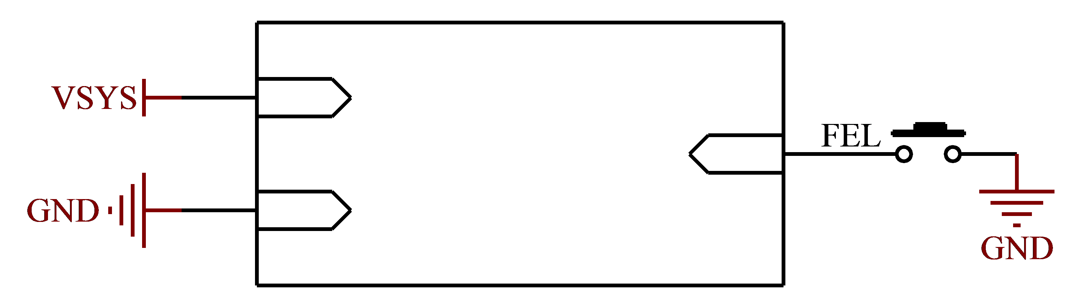
Please refer to “Appendix IV. for the minimal system schematic diagram However, in most cases, it is recommended to connect some external devices in addition to the minimal system, such as a debugging serial port, otherwise, the user can not check whether the system is booted. After completing these steps, additional user-specific functions can be added based on the default interface definitions provided by Forlinx for the SoM.
Please refer to section 3.5 in “Chapter 3.OK62xx-C Carrier Board Description” for the peripheral circuits.
3. OK62xx-C Development Platform Description
3.1 OK62xx-C Development Board Interface Diagram
The SoM and carrier board of the Forlinx OK62xx - C development platform are connected via board-to-board connectors. Since the carrier board is compatible with multiple SoMs from the AM62 series, the term “OK62xx - C” appears in the PCB silkscreen and when referring to the development board name in this document, representing the CPU series that this product is compatible with. The main interfaces are shown in the following figure:

3.2 OK62xx-C Development Board Dimension Diagram
PCB Size: 190mm × 130mm
Fixed hole size: spacing: 180mm × 120mm, hole diameter: 3.2mm.
Plate making process: thickness 1.6mm, 4-layer PCB.
Two mounting holes with a diameter of 3.2mm are reserved on the carrier board. You can select and install the heat sink according to the site environment. Please add a layer of insulated heat-conducting silicone pad on the contact surface between the heat sink and the core board. 38Mm×38mm×10mm. For more detailed dimensions, please refer to the following figure.
3.3 Carrier Board Naming Rules
A-B-C+DEF:G
Field |
Field Description |
Value |
Description |
|---|---|---|---|
A |
Product Line Identification |
OK |
Forlinx Embedded development board |
- |
Segment Identification |
- |
When the first digit of the CPU value is a letter, |
B |
CPU Name |
62xx |
xx stands for the same carrier board that can be |
- |
Segment Identification |
- |
Parameter segment sign |
C |
Connection |
C |
Board to Board Connector |
+ |
Segment Identification |
+ |
The configuration parameter section follows this identifier. |
D |
Type |
M |
Carrier board(Note: carrier board identification M, not filled by default) |
E |
Operating Temperature |
I |
-40 to 85℃ industrial level |
F |
PCB Version |
12 |
V2.2 |
: |
Internal Identification of the Manufacturer |
: |
This is the internal identification of the manufacturer |
G |
Connector origin |
1 |
Imported connector |
3.4 Carrier Board Resources
Function |
Quantity |
Parameter |
|---|---|---|
LVDS |
2 |
Dual asynchronous channels (8 data, 2clocks) support 1920x1200p60, |
16-bit RGB parallel interface |
1 |
The 16 bit data interface led out from the FPC socket on the carrier board |
Camera |
1 |
The MIPI CSI signal is led out from the carrier board through the FPC seat |
Ethernet |
2 |
Supports 10/100/1000Mbps self-adaption, which is led out through RJ45 |
USB2.0 |
4 |
3 x USB HOST |
DEBUG UART |
3 |
The UART0 in the main domain and the WKUP_UART0 in the R5 domain |
RS485 |
1 |
Electrical quarantine, automatically control the direction of sending and receiving |
SPI |
1 |
MCU _ SPI0 is clocked at up to 50 MHz through a 2.54 mm pitch pin header |
I2C |
2 |
MCU _ I2C0 and WKUP _ I2C0 are led out through a 2.54 mm pitch header |
GPMC |
1 |
GPMC _ AD0 ~ AD15 16-bit data signals and corresponding control |
CAN-FD |
1 |
Electrical quarantine supporting CAN-FD, speed up to 5Mbps |
Audio |
1 |
Supports 1 x headphone output, 2 x speaker output and 1 x MIC input. |
TF-CARD |
1 |
Supports 1 x TF for UHS - I TF cards, up to 104MB/s. |
4G/5G |
1 |
You can choose either the 4G or 5G function. |
WiFi |
1 |
Default on-board AW-CM358M; |
Bluetooth |
1 |
|
KEY |
5 |
A core 4 key inputs M core 1 key input |
LED |
8 |
A and 4 LED outputs M Core 4 LED outputs |
RTC |
1 |
On-board independent RTC chip, which can record time via a button |
EEPROM |
1 |
2K bit capacity is mounted to MCU _ I2C0 or WKUP _ I2C0 optionally |
QSPI Flash |
1 |
The capacity is 128M bit, which can be mounted to QSPI or MCU _ SPI0 |
JTAG |
1 |
Led out via 2 X 10Pin double row 1.27 mm pitch socket |
Note:
“TBD” means the function has not been developed in this phase;
The parameters in the table are hardware design or theoretical CPU values.
3.5 OK62xx -C Carrier Board Description
Note: The component UID with “_DNP” mark in the diagram below represents it is not soldered by default
3.5.1 Carrier Board Power
It uses a 12V power adapter for the power supply, and the power connector is a DC005 socket. S1(dip switch) is the power switch, which moves according to the screen printing indication on the board. The rear of S1 has TVS for electrostatic protection, F1 for over-current protection, and D1 and F1 cooperate for anti-reverse connection protection.
VCC_12V is decreased to VCC_5V via U1. VCC_5V directly powers the SoM to ensure that it can be powered on first.
VCC_5V is decreased to VCC_3V3 via U2 U2 is controlled by the POWER_EN signal of the SoM (this signal is an open-drain output, pulled up to the 3.3V of the SoM through a 100K resistor, and this signal is released after the key power supply of the SoM is powered on). VCC_3V3 supplies power to all 3.3V power-consuming devices on the carrier board.
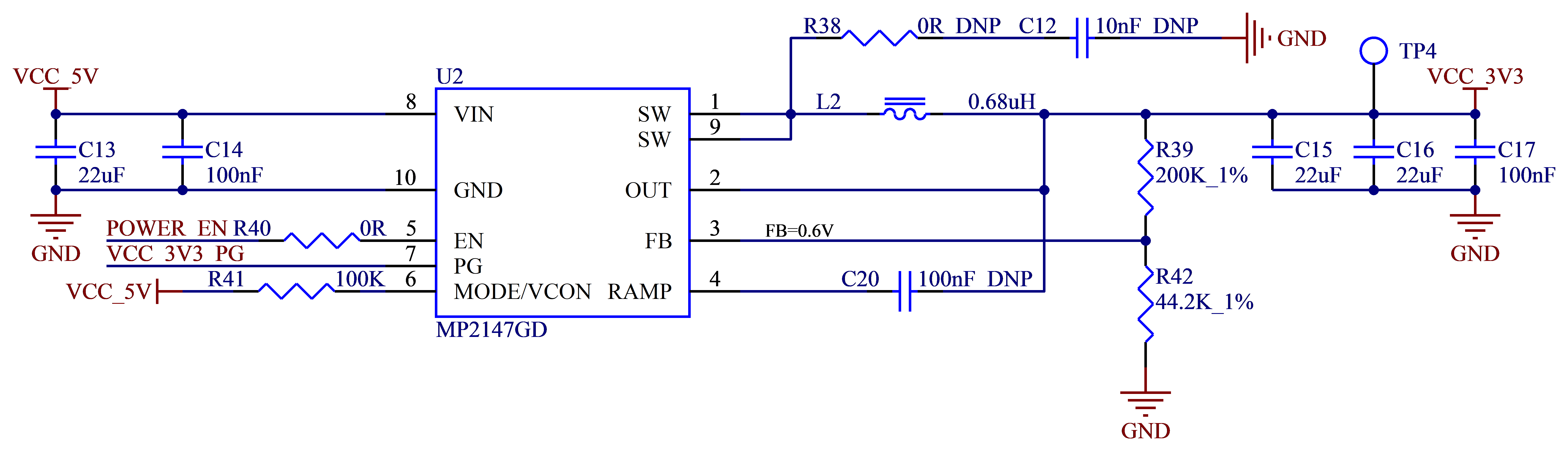
VCC_5V outputs VDD_5V in a controlled manner through U4. U4 is controlled by the PG signal of U2. After VCC_3V3 is powered on, U4 conducts. VDD_5V powers some 5V - powered devices on the carrier board.
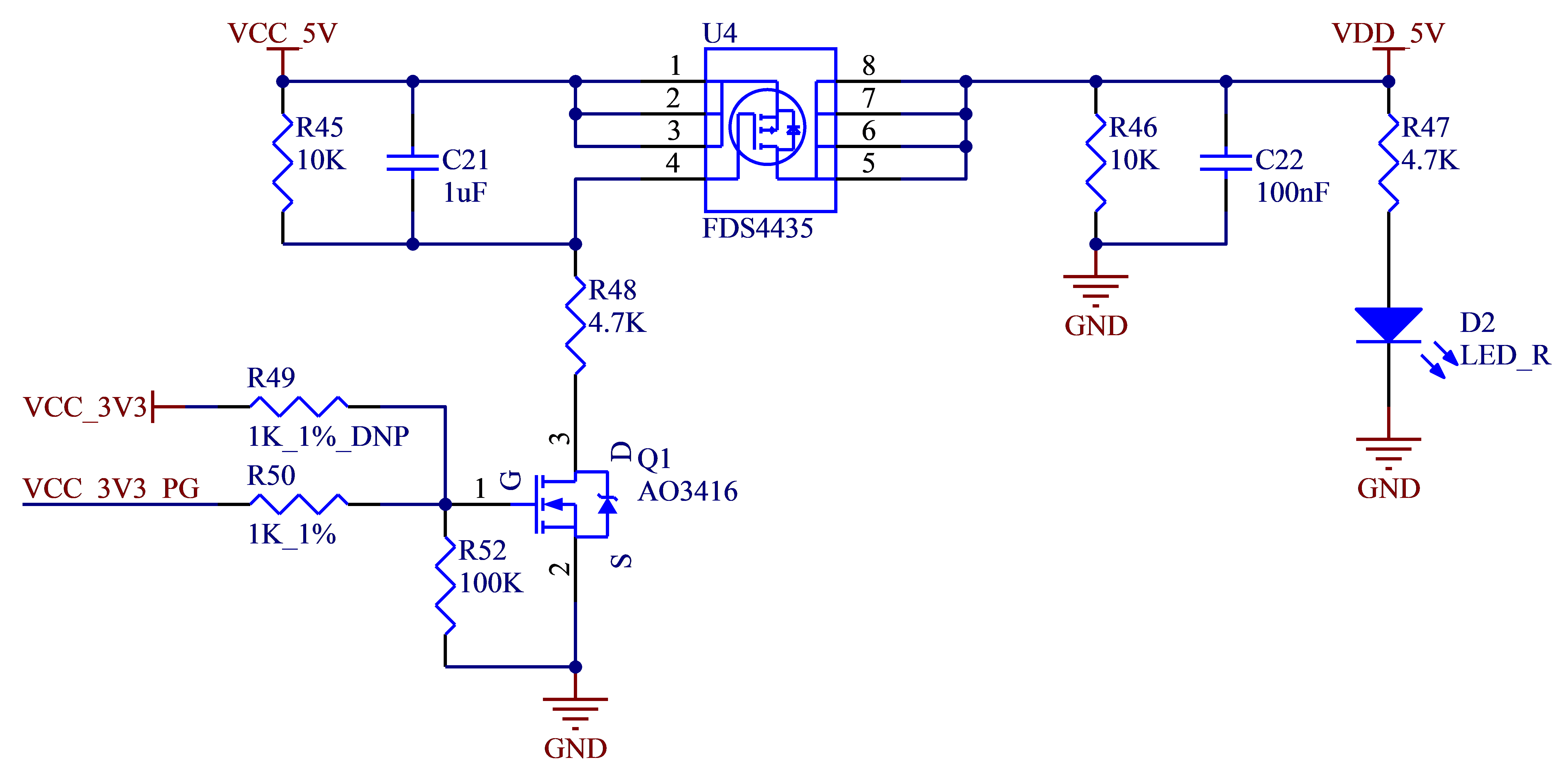
VCC_3V3 is stepped down to VCC_1V8 through U5 to supply power to the 1.8V power-consuming devices on the carrier board.
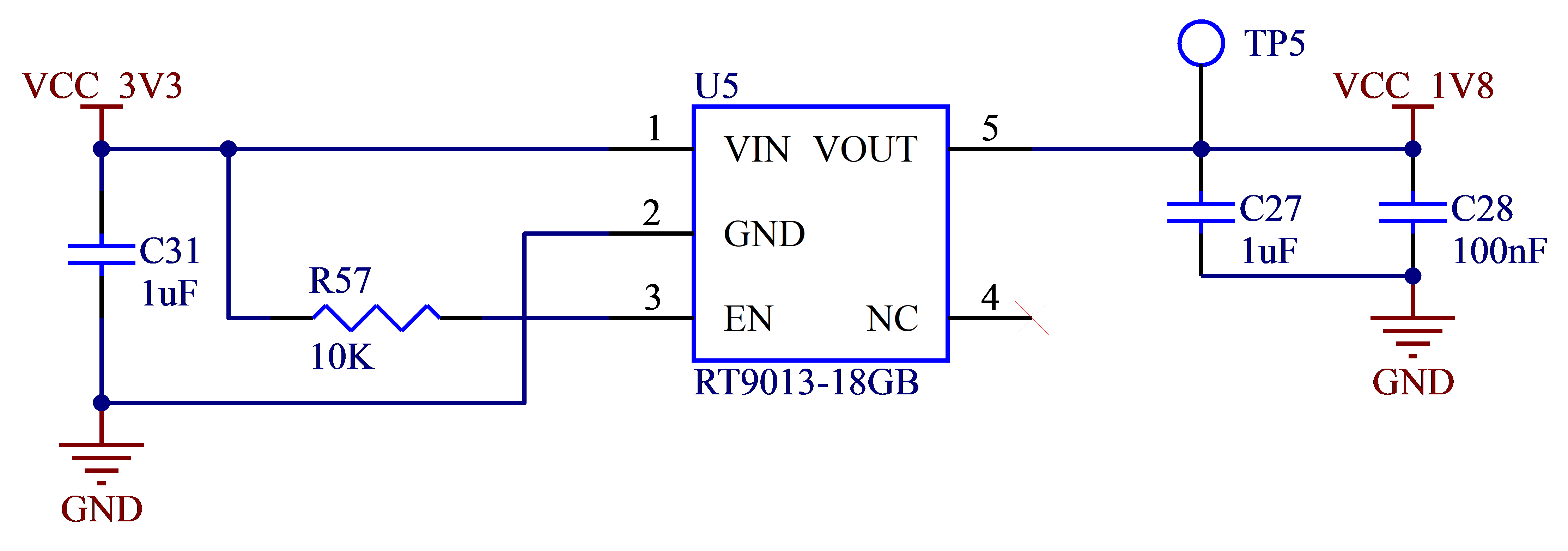
VCC_5V is stepped down to VCC_3V3_TOUCH through U6 to supply power to the resistive touch chip. It should be noted that VCC_3V3_TOUCH and the SoM need to be powered on simultaneously to meet the power-on sequence requirements of TS2007.
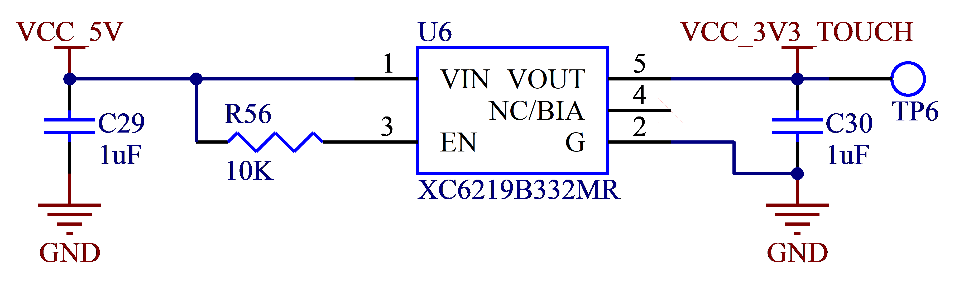
Note:
When designing by yourself, please ensure the power-on sequence of the power supply;
Refer to the corresponding chip manual for the component selection and external layout of the step-up and step-down chip to ensure a good power circuit.
3.5.2 Reset Signal
RESET_REQZ is the reset signal input for the SoM. For ease of debugging, it is connected to a button.
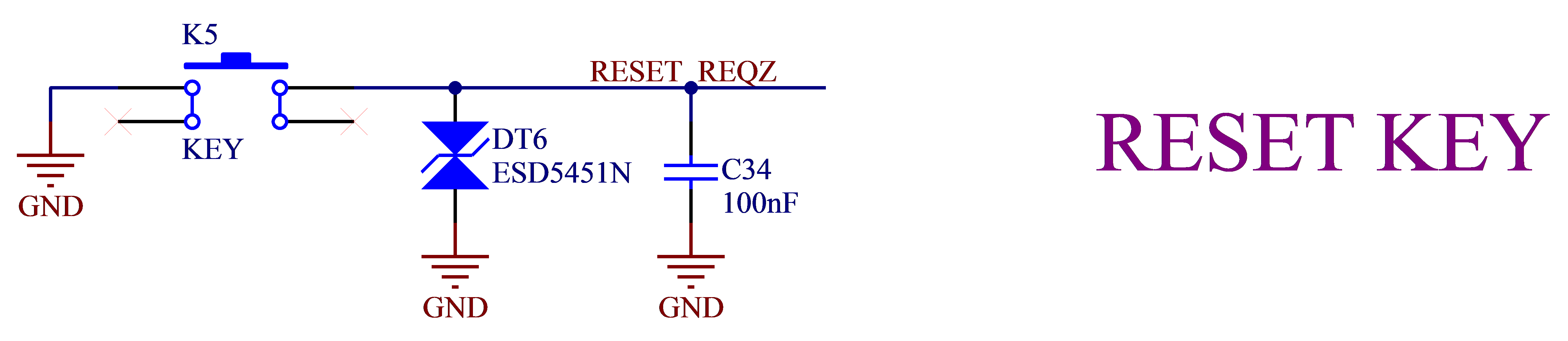
Note: RESET_REQZ can only reset the A core. If you need to reset both the A core and the M core simultaneously, it is recommended to use the MCU_RESETz (RU37) pin.
3.5.3 Boot Configuration
GPMC0 _ AD0 ~ GPMC0 _ AD15 of the SoM correspond to BOOTMODE00 ~ BOOTMODE15 respectively.
BOOTMODE Pin Mapping:
15 |
14 |
13 |
12 |
11 |
10 |
9 |
8 |
7 |
6 |
5 |
4 |
3 |
2 |
1 |
0 |
|---|---|---|---|---|---|---|---|---|---|---|---|---|---|---|---|
Reserved |
Reserved |
BackupBoot Mode Config |
Backup Boot Mode |
Primary Boot Mode Config |
Primary Boot Mode |
PLL Config |
BOOTMODE[02:00]: Configuration related to the CPU PLL. On the core board,
it is configured as BOOTMODE[02:00] = 011.
There is no need to repeat the configuration on the baseboard.

BOOTMODE[03:06]: Requested boot (primary) mode after POR, that is,
the peripheral/memory from which to boot.
The default configuration on the core board is BOOTMODE[03:06] = 0001.

BOOTMODE[07:09]: These pins provide optional configurations for the primary boot
and are used in combination with the selected boot mode.
The default configuration on the core board is BOOTMODE[07:09] = 000.

BOOTMODE[10:12]: Select the backup boot mode, that is, if the primary boot device fails,
boot from the backup peripheral/memory.
The default configuration on the core board is BOOTMODE[10:12] = 011.

BOOTMODE[13]: Optional configuration for the backup boot mode, used in combination with
the selected boot mode. The default configuration on the core board is BOOTMODE[13]: 0.

BOOTMODE[14:15]: Reserved pins. The default configuration on the core board is
BOOTMODE[14:15] = 00.

The following table shows the Primary Boot Mode Selection:
Primary Boot Mode Config |
Primary Boot Mode |
||||||
|---|---|---|---|---|---|---|---|
B9 |
B8 |
B7 |
B6 |
B5 |
B4 |
B3 |
|
Reserved |
Read Mode2 |
Read Mode1 |
0 |
0 |
0 |
0 |
Serial NAND |
Reserved |
Iclk |
Csel |
0 |
0 |
0 |
1 |
OSPI |
Reserved |
Iclk |
Csel |
0 |
0 |
1 |
0 |
QSPI |
Reserved |
Mode |
Csel |
0 |
0 |
1 |
1 |
SPI |
Clkout |
0 |
Link Info |
0 |
1 |
0 |
0 |
Ethernet RGMII |
Clkout |
Clk src |
0 |
0 |
1 |
0 |
1 |
Ethernet RMII |
Bus reseet |
Reserved |
Ader |
0 |
1 |
1 |
0 |
I2C |
Reserved |
Reserved |
Reserved |
0 |
1 |
1 |
1 |
UART |
1 |
Reserved |
Fs/raw |
1 |
0 |
0 |
0 |
MMCSD Boot(SD Card Boot or eMMC Boot using UDA) |
Reserved |
Reserved |
Reserved |
1 |
0 |
0 |
1 |
eMMC Boot |
Core Volt |
Mode |
Lane Swap |
1 |
0 |
1 |
0 |
USB |
Reserved |
Reserved |
Reserved |
1 |
0 |
1 |
1 |
GPMC NAND |
Reserved |
Reserved |
Reserved |
1 |
1 |
0 |
0 |
GPMC NOR |
Reserved |
Reserved |
Reserved |
1 |
1 |
0 |
1 |
Reserved |
SFPD |
Read Cmd |
Mode |
1 |
1 |
1 |
0 |
Xspi |
Reserved |
ARM/Thumb |
No/Dev |
1 |
1 |
1 |
1 |
No-boot/Dev boot |
The OK62xx-C carrier board is compatible with multiple starting modes through the DIP switch S2, as shown in the figure below:
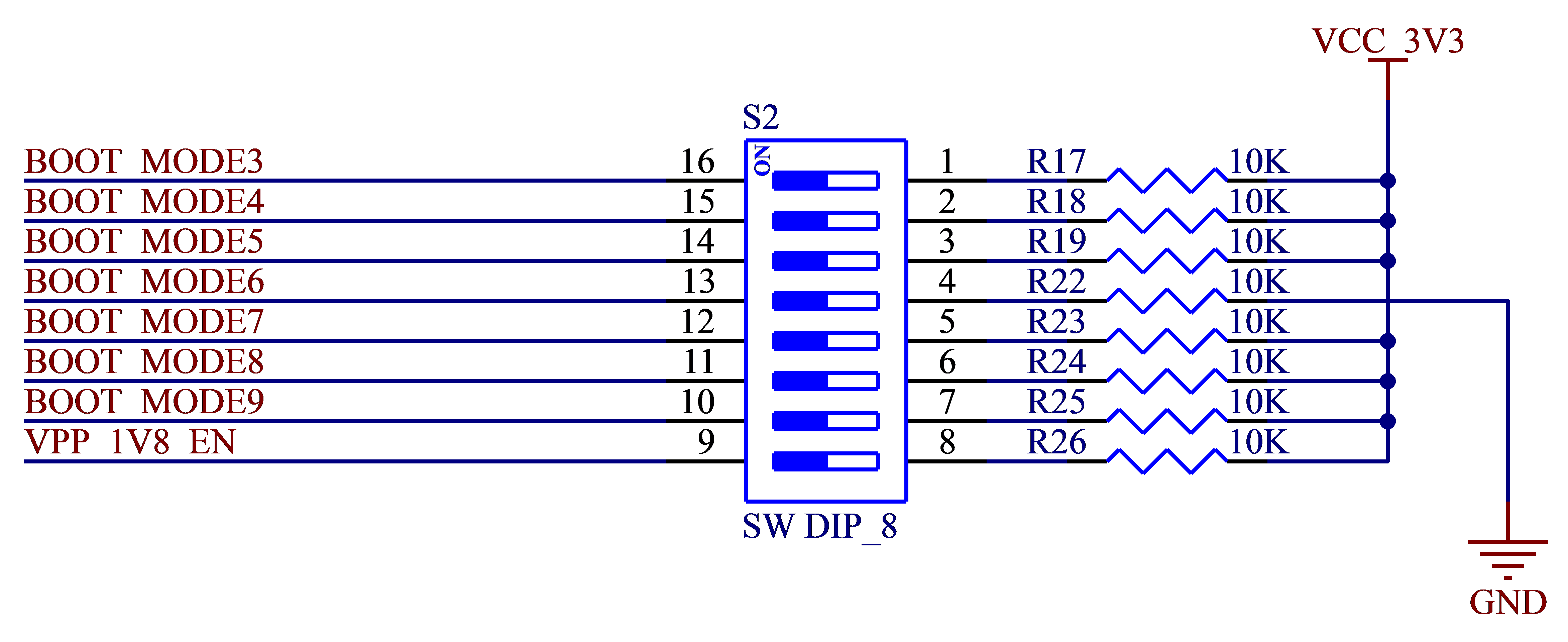
The following table shows the correspondence between the startup modes of the SoM and the DIP switches. “ON” and “OFF” indicate the toggling directions of the DIP switches. “S2 order” refers to the serial numbers of the DIP switches. On the PCB, there are markings from 1 to 8 above S2, where the 8th bit has nothing to do with startup. In the schematic diagram, “S2 order” corresponds to pins 1 to 8 of S2 respectively.
Boot Media |
S2 Order |
||||||
|---|---|---|---|---|---|---|---|
1 |
2 |
3 |
4 |
5 |
6 |
7 |
|
eMMC |
OFF |
OFF |
OFF |
OFF |
OFF |
OFF |
OFF |
TF Card |
OFF |
OFF |
OFF |
OFF |
OFF |
OFF |
ON |
QSPI Flash |
ON |
ON |
OFF |
ON |
OFF |
ON |
OFF |
USB Disk |
OFF |
ON |
OFF |
OFF |
OFF |
ON |
OFF |
USB DFU |
OFF |
ON |
OFF |
OFF |
OFF |
OFF |
OFF |
Note:
When designing the carrier board, please pay attention to the default configuration of the BOOTMODE configuration pins on the SoM and correctly configure the boot mode. Otherwise, the system may fail to start; The pins GPMC0_AD0 - GPMC0_AD15 are all boot - option pins. When there are sufficient pins, it is not recommended to use them for other functions. If they must be used, it is recommended to add a buffer circuit to prevent affecting the reading of boot options;
It is not recommended to use USB Disk for flashing. When the processor is in the USB Disk boot mode, its compatibility with USB flash drives is poor, which may lead to flashing failure. The processor errata are described as follows:
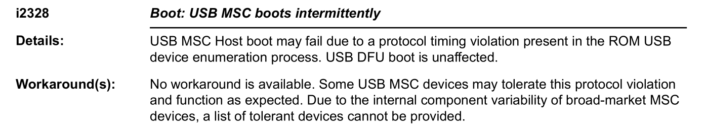
3.5.4 Debugging Serial Port
The debugging serial port uses a TYPE-C interface. The XR21V1414 chip integrates three serial ports into one USB bus, enabling simultaneous debugging of three cores.
The debug signals from the SoM pass through a buffer chip and a conversion chip before reaching the TYPE-C interface. This design prevents leakage current to the SoM or carrier board when plugging in the debug cable while the carrier board is powered off.
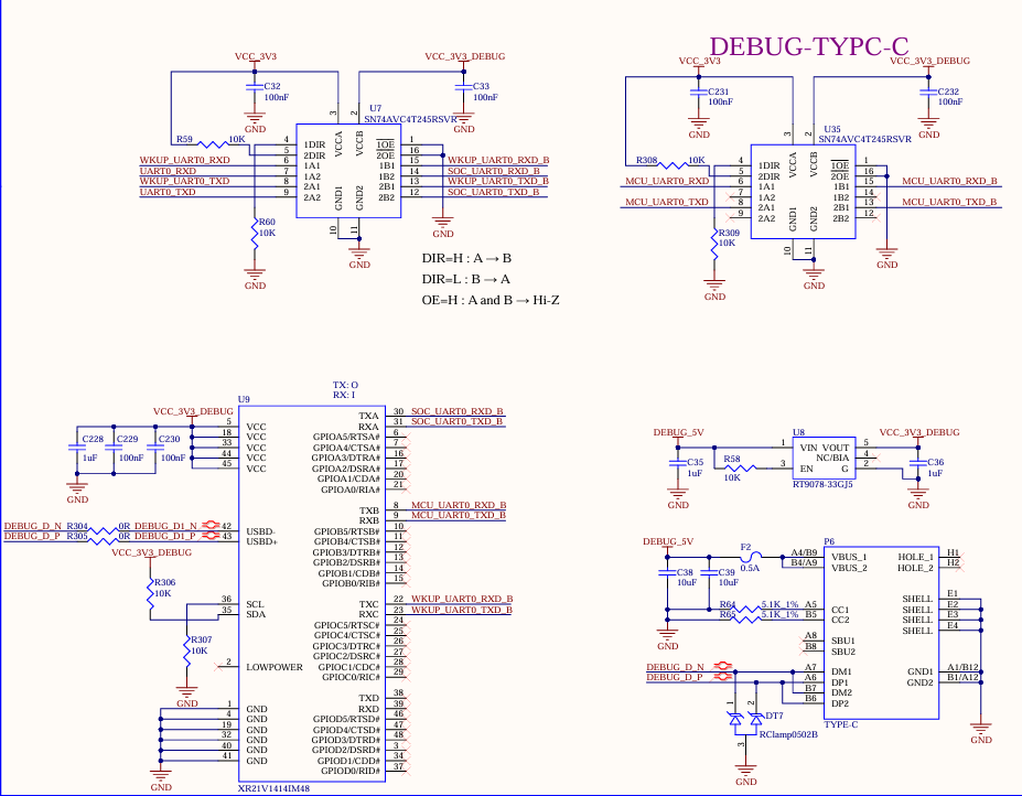
Note:
For the convenience of later debugging, please lead out the debugging serial port when designing the carrier board;
U7 is only a reference circuit. Users can also use other circuits such as MOS to prevent reverse current flow;
U9 is powered by the VBUS of the Type - C interface, which can ensure that the PC loads the driver in time and guarantee the integrity of the printed information.
3.5.5 JTAG
The JTAG of the carrier board is a TI standard circuit, which can be directly plugged into a TI emulator to simulate the SoM.
3.5.6 User LED and Button
The development board divides the user LEDs and user buttons into two domains, namely the Main domain and the MCU domain, corresponding to the relevant GPIOs of the Main and MCU domains of the SoM.
The Main domain integrates user LEDs and user buttons together, facilitating users to test the input and output functions of GPIO. It should be noted that when testing the GPIO output function, do not press the key, otherwise the GPIO will be forced to a low level. The following figure shows the principle of the Main domain:
The MCU domain is designed with 1 x user key input and 4 x user LED. The following figure shows the principle of MCU domain:

3.5.7 Display Interface
The SoM supports dual LVDS and single RGB parallel interface outputs.
Among them, the dual - channel LVDS is led out through the P16 2x19P 2.0mm pitch double - row pin header, which is default - adapted to the Forlinx 10.1 - inch LVDS screen.
The single-channel RGB parallel interface (RGB 565 16bit bus by default) is led out through the P14 54P 0.5mm pitch FPC seat, which is suitable for the 7-inch LCD screen of Forlinx by default.

The reset and interrupt signals of the touchpad for the 7-inch LCD screen and the 10.1-inch LVDS screen are at 3.3 V level, while the four GPIOs of the CPU are at 1.8 V level, so level conversion is required, and the signal flow is bidirectional.
Note:
Correctly allocate RGB signals;
It is recommended not to mount the touch chips of the LCD and LVDS on the same group of IIC;
Impedance requirements: Single-ended 50ohm;
Differential: 100 ohm.
3.5.8 Video Input Interface
The SoM supports 1 x MIPI DPHY 4Lanes input interface. 4 Lanes are led out for standby through the P15 2x10P 2.0mm pitch double-row pin header from the development board, and 2Lanes are led out through the P13 26P 0.5mm pitch FPC socket, which is adapted to the Forlinx OV5645 camera module.
Note:
Pay attention to the level matching of IIC;
The power supply of the camera needs to be filtered with a magnetic bead;
Impedance requirements: Differential: 100 ohm.
3.5.9 TF Card
The carrier board P7 is a TF Card interface, which can support system boot and burn.

Note:
The power supply for the TF card must be controlled; refer to the carrier board circuit for implementation;
Impedance requirements: Single-ended 50ohm.
3.5.10 Ethernet Interface
The carrier board supports dual 1000/100/10M Ethernet interfaces, which are led out via RJ45.
Note:
Note that the RGMII IO level is 3.3V, and the interface level at the PHY chip end needs to be set consistently;
The PCB Layout needs to ensure the integrity of the RGMII signal reference plane and the integrity of the power supply reference plane around the PHY chip;
2 x PHY are mounted on the same group of MDC MDIO interfaces, so attention should be paid to avoid conflicts in PHY addresses;
Equivalent length requirement: the receiving and sending of RGMII can be grouped into equal lengths, with an equal length requirement ≤ 12.5 mil;
**Impedance requirement: 50 ohm. **
3.5.11 USB Interface
The SoM supports 2 x USB2.0. Among them, USB1 expands 3 x USB2.0 Host through a HUB chip and is led out through 3 x USB sockets P19, P20, and P21.
USB0 is configured in OTG mode and is led out through Type - C. The master - slave mode is selected through the DIP switch S3. When S3 is switched to OFF, the SoM is in Device mode; when switched to ON, the SoM is in Host mode.
Note:
ESD protection devices need to be added to the data line;
Impedance requirements: Differential 90 ohm.
3.5.12 4G&5G
The P24 M.2 Key - B socket on the carrier board can be plugged with 4G and 5G modules, but they cannot be used simultaneously. P31 is the SIM card socket.
3.5.13 WIFI&BT
The carrier board is designed with a CAM358 WIFI & BT module, which can realize WIFI & BT functions.
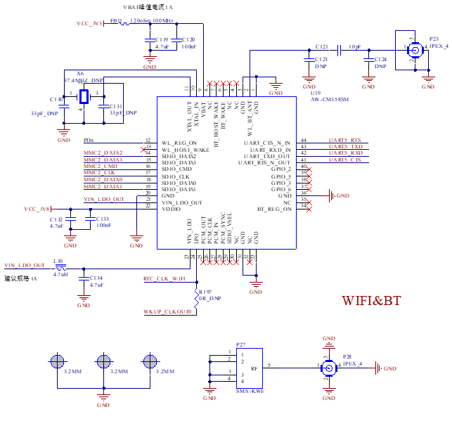
Note: Impedance requirement: 50 ohm.
3.5.14 Audio Interface
The development board features one HP/MIC port and two SPK ports.
HP/MIC Port: A 4-pole headphone jack supports both playback and recording functions. It also features plug detection, which automatically switches audio output from the speaker (SPK) channels to the headphone when a headphone is plugged in.
SPK Ports: Two speaker ports are implemented via 2.54mm-pitch white terminal blocks.
The on-board audio codec NAU88C22 integrates a Class-D amplifier capable of driving two 8Ω speakers with a maximum output power of 1W.
For applications requiring higher external amplifier power, note that:
The audio signal must be sourced from the headphone socket, not the speaker terminals.
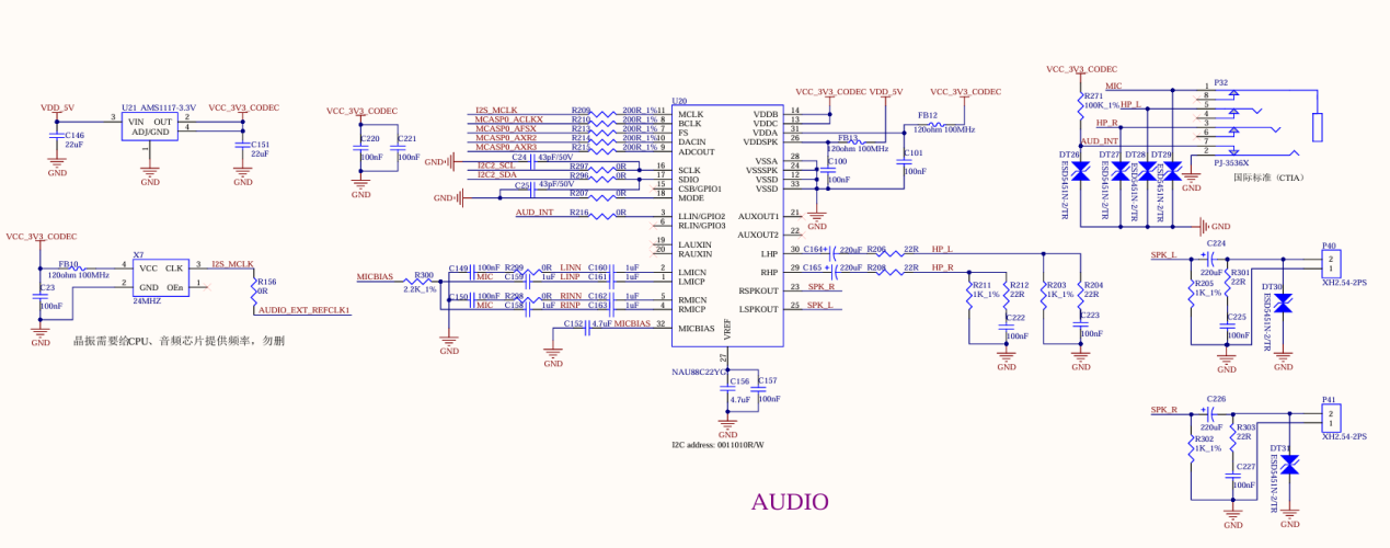
Note:
In PCB layout, the return current paths for analog and digital signals must be separated to prevent crosstalk;
The speaker is powered by a Class D amplifier, not a traditional analog amplifier;
Each speaker must be connected to its own dedicated socket. Do not share speaker wires between sockets, and do not connect the speaker signal lines to the ground plane.
3.5.15 RTC
External RTC is integrated on the carrier board, and the power supply battery is CR2032.
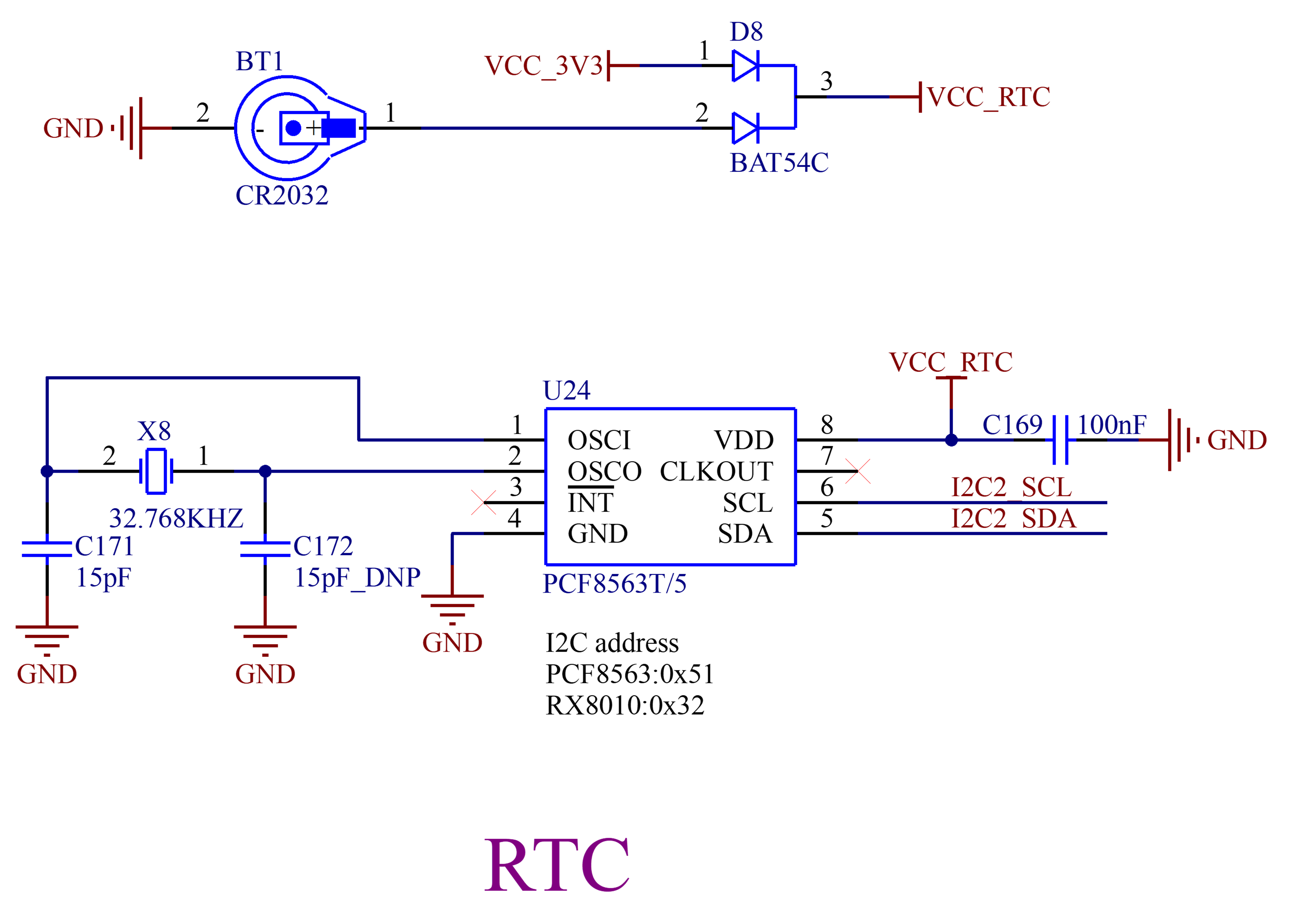
3.5.16 QSPI Flash
The QSPI Flash is integrated on the carrier board, and the Main domain and the MCU domain select who mounts the Flash by means of jumpers.
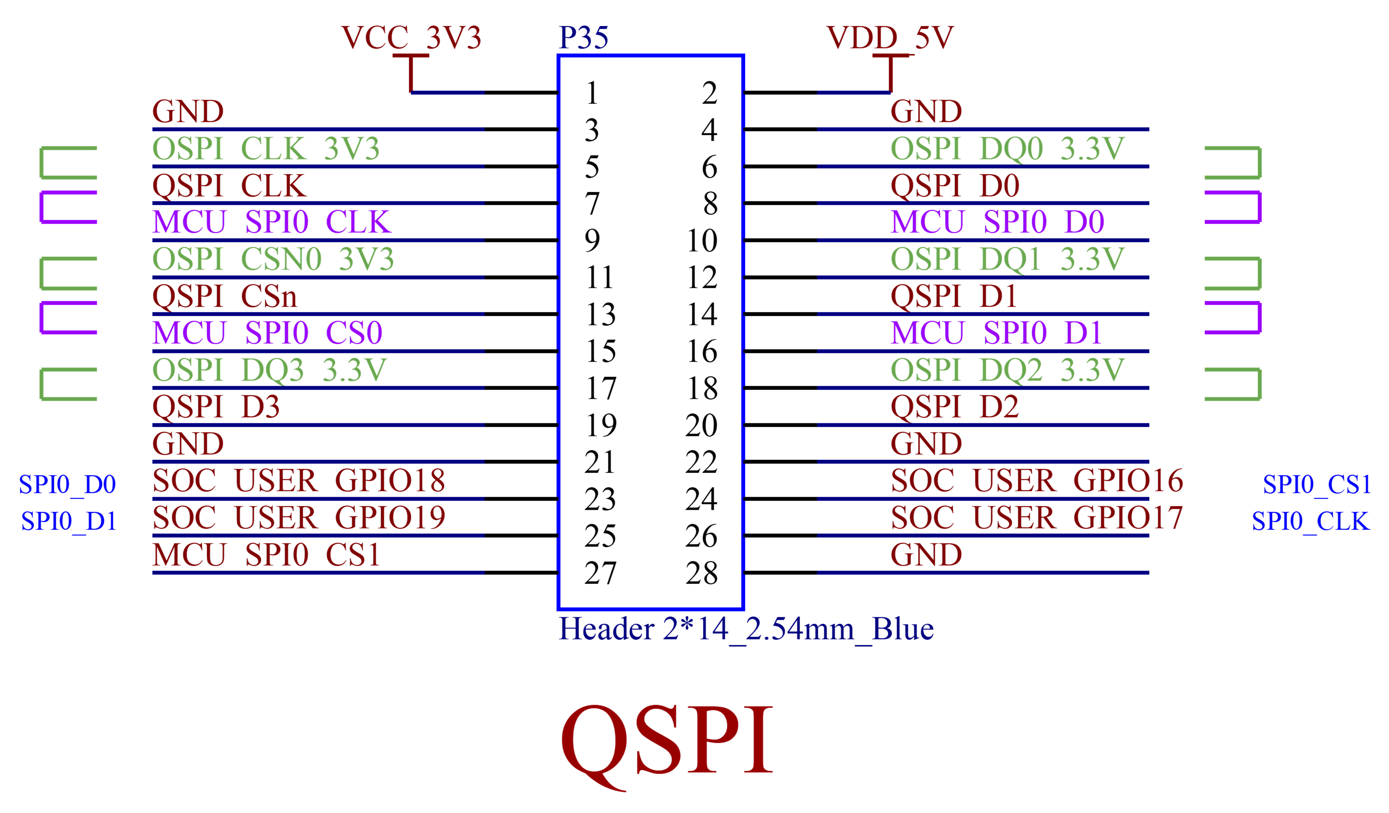
3.5.17 GPMC Interface
A part of the GPMC signals are led out through the P34 2x14 2.54mm pitch double - row pin header from the development board, supporting the 16 - bit address - data multiplexing mode.
3.5.18 CAN&RS485
2 x CAN FD and 1 x RS485 are integrated on the carrier board. The 2 x CAN FD belongs to the Main domain and the MCU domain respectively.
Note:
The CAN and 485 signals of this development board need to undergo relevant EMC tests, and a large number of protection measures need to be added. If you have no relevant requirements or the test requirements are of a low level, please make deletions according to the scheme by yourselves;
Please refer to the development board for the ground isolation part.
3.5.19 EEPROM
An EEPROM is integrated on the carrier board. The MCU and the WKUP domain can select which one mounts the EEPROM through a jumper.
3.5.20 MCU User-defined Pins
A part of the MCU Pins are led out through the P36 2x14 2.54mm pitch double - row pin header from the development board.
4. Hardware Design Guide
Power:
When designing the carrier board, it is necessary to strictly follow the rule that the SoM is powered on first, and the VCC_3V3_SYS_PG output from the SoM controls the power - on of the carrier board;
When the functional pins of the SoM directly communicate with peripherals, attention should be paid to the reverse current flow issue. That is, when the SoM is not powered on and the peripheral is powered on first, there is a certain risk of reverse current flowing into the SoM, which may affect the startup of the SoM. In this case, the power - on sequence of the peripherals should be controlled or a reverse - current prevention circuit should be added;
Some pins of the SoM have a level of 1.8V, and attention should be paid to level matching;
The power supply of the TF card needs to be controlled;
The display interface and USB interface devices have relatively high power consumption. Attention should be paid to PCB wiring and the corresponding over - current protection circuit;
Network PHY chips usually have multiple power - supply pins, such as AVDD, DVDD, DCDD_RGMII, etc. The required voltage of each power - supply path needs to be checked. Moreover, magnetic beads are usually needed for filtering, and attention should be paid to ensuring that the value and quantity of bypass capacitors meet the requirements;
The power supply of 4G and 5G modules needs to meet the requirements. It is recommended that the power - supply voltage of the 5G module be 4.2V;
Usually, the pin level of SDIO and UART of WIFI & BT module is 1.8 V, and it is necessary to check whether the pin level is matched;
If quarantine is required for CAN-RS485, quarantine is required for both signal and power.
Reset Signal:
The following figure shows the reset block diagram of the CPU:
5. OK62xx - C Development Board Linux System Whole - Machine Power Consumption Table
AM6254:
Hardware |
Test Item |
Power voltage (V) |
Current |
|
|---|---|---|---|---|
Transient Peak Value |
Stable Value |
|||
Development Board |
Power-on start without load |
12 |
246 |
180 |
On-load LVDS + LCD |
12 |
602 |
562 |
|
On-load LVDS+LCD+cpu the usage rate is 90% |
12 |
753 |
743 |
|
Single SoM |
Power-on start without load |
5 |
440 |
295 |
The CPU usage rate is 100%. |
5 |
- |
415 |
AM6232:
Hardware |
Test Item |
Power voltage (V) |
Current |
|
|---|---|---|---|---|
Transient Peak Value |
Stable Value |
|||
Development Board |
Power-on start without load |
12 |
237 |
182 |
On-load LVDS + LCD |
12 |
585 |
543 |
|
On-load LVDS+LCD+cpu the usage rate is 90% |
12 |
734 |
724 |
|
Single SoM |
Power-on start without load |
5 |
420 |
300 |
The CPU usage rate is 100%. |
5 |
- |
370 |
AM6231:
Hardware |
Test Item |
Power voltage (V) |
Current |
|
|---|---|---|---|---|
Transient Peak Value |
Stable Value |
|||
Development Board |
Power-on start without load |
12 |
223 |
183 |
On-load LVDS + LCD |
12 |
578 |
538 |
|
On-load LVDS+LCD+cpu the usage rate is 90% |
12 |
728 |
717 |
|
Single SoM |
Power-on start without load |
5 |
382 |
310 |
The CPU usage rate is 100%. |
5 |
- |
355 |
Note:
Peak Current: Maximum current value during booting;
Stable Value: Current value stays on the boot screen after booting.
6. Connector Dimension Diagram
SoM Connector Dimension:
Carrier board Connector Dimension:
7. Minimum System Schematic
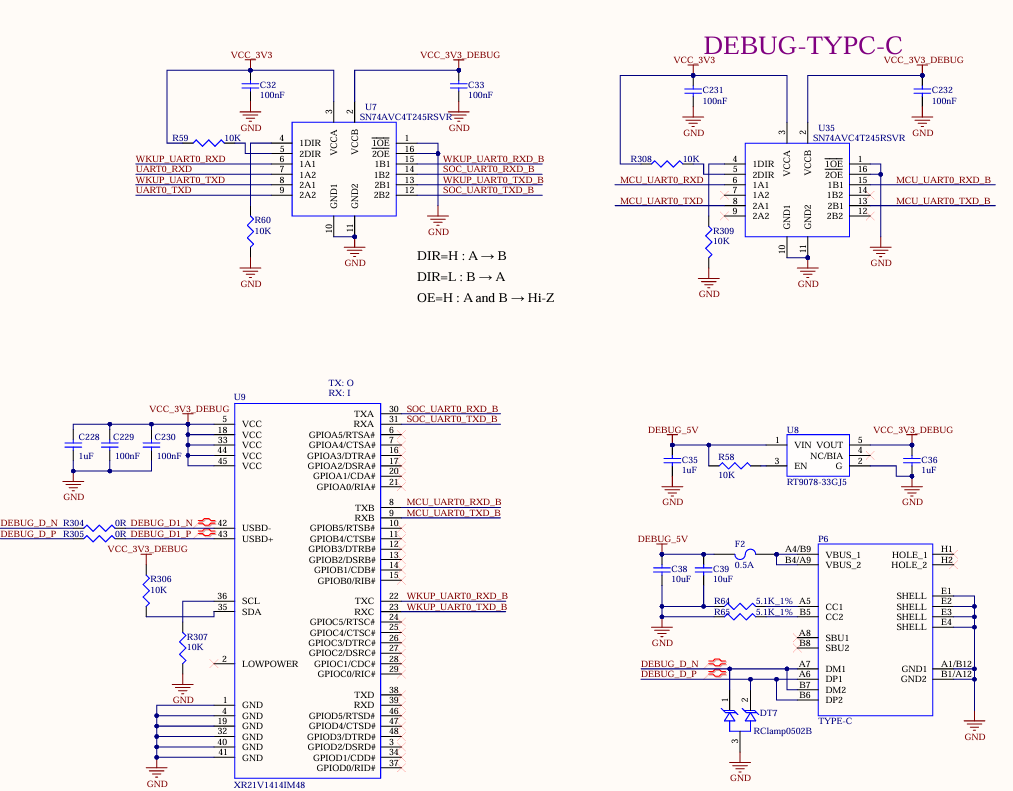
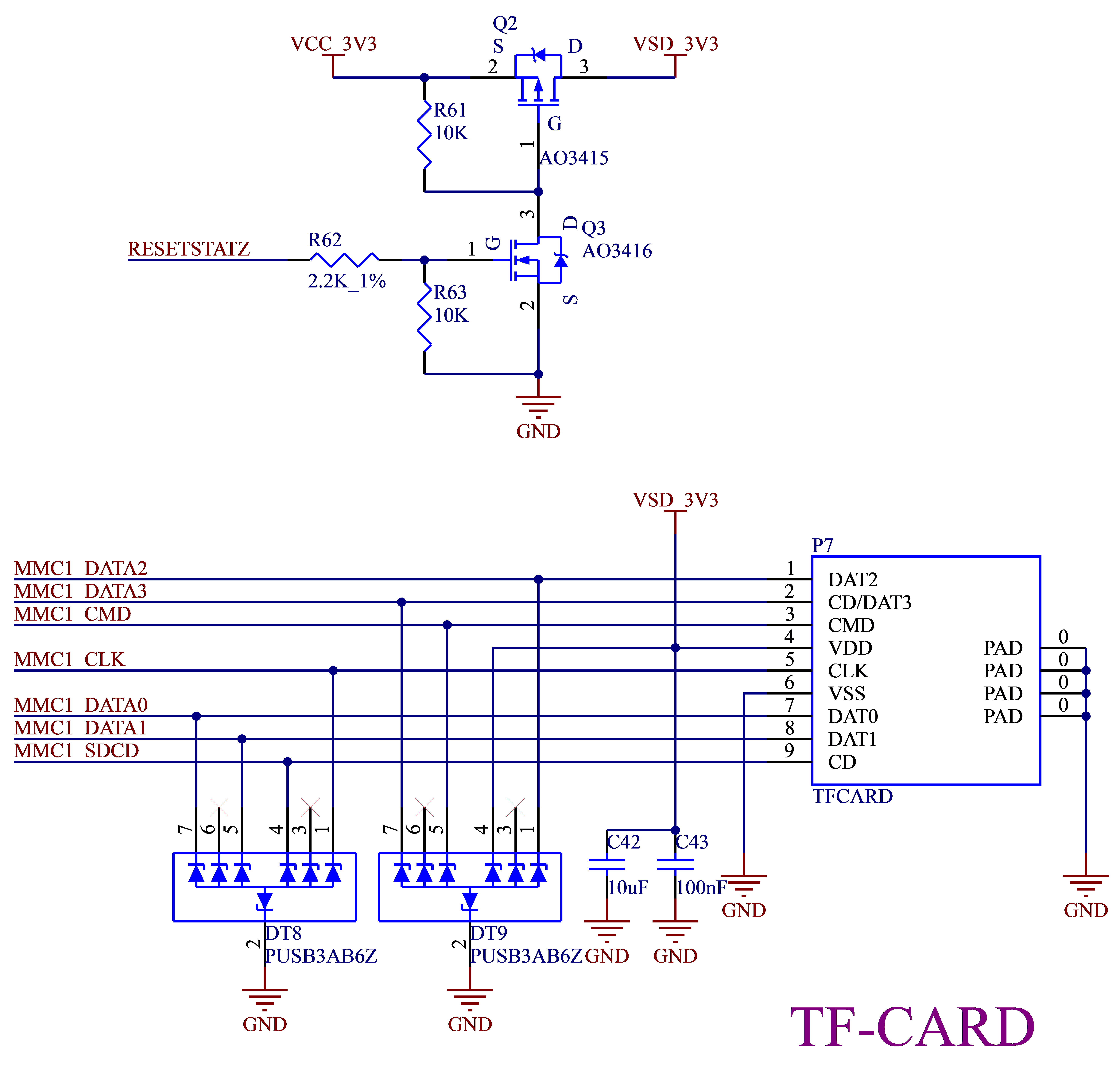
Note:
Note: The minimum system includes SoM power supply, system flash circuit, and debugging serial port circuit.