User’s Hardware Design Guide_V1.0
Document classification: □ Top secret □ Secret □ Internal information ■ Open
Copyright
The copyright of this manual belongs to Baoding Folinx Embedded Technology Co., Ltd. Without the written permission of our company, no organizations or individuals have the right to copy, distribute, or reproduce any part of this manual in any form, and violators will be held legally responsible.
Forlinx adheres to copyrights of all graphics and texts used in all publications in original or license-free forms. The drivers and utilities used for the components are subject to the copyrights of the respective manufacturers. The license conditions of the respective manufacturer are to be adhered to. Related license expenses for the operating system and applications should be calculated/declared separately by the related party or its representatives.
Overview
This document corresponds to the UP4 SoM product, describing the schematic design of the UP4 peripheral circuits, PCB design, troubleshooting approaches for common interface issues, design features of functional interfaces, and more. It assists engineers in quickly familiarizing themselves with the product, facilitating maintenance and development tasks.
The designs provided in this document are for guidance only. During application design, please adapt your designs based on actual scenarios and conditions. For any inquiries, please contact our company’s technical support.
Application Scope
This hardware manual applies to the UP4 Forlinx SoM
Revision History
Date |
Version |
Revision History |
|---|---|---|
02/03/2026 |
V1.0 |
Initial Version |
1. Schematic Design
1.1 Schematic Design Guidelines for UP4 Carrier Board
All pins must be designed according to the voltage levels specified in the UP4 Pin Definition Table. Pins without special requirements below can be directly connected, provided the voltage levels are compatible.
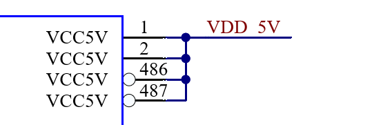
1. Pin (1/2) Signal Name (VCC5V) Design Requirements
The main power supply pins for the SoM on the carrier board must use a non-switched 5V power source from the carrier board. It is capable of delivering 3A (15W) dedicated to the SoM alone. If the carrier board also utilizes this power source, the total required current must be the sum of 3A plus the carrier board’s current demand. Additionally, a redundancy margin of at least 20% of the system’s (SoM + carrier board) peak power consumption must be ensured. Therefore, the 5V power source should provide power ≥ (15W + Carrier board peak power) * 120%. Filter capacitors must be added on the carrier board before this 5V signal is supplied to the SoM. Recommended capacitor values are 100nF, 1uF, 10uF, and 22uF.
Diagram:
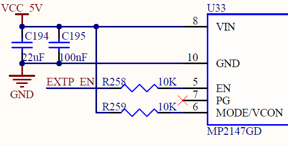
2. Pin (4) Signal Name (EXTP_EN) Design Requirements
When designing the carrier board, use this pin to control the power-up sequence of the carrier board’s switched power supplies. This pin is configured as push-pull output on the SoM. The carrier board must have a pull-down resistor to ensure a default low state, keeping the carrier board’s controlled power supplies off by default. They should only power up after the SoM outputs a high signal on this pin. The controlled power supplies on the carrier board must have soft-start functionality to avoid inrush current spikes during power-up.
Design Reference:
1. Control the Power MOSFET to Turn on the Carrier Board’s Controlled Power Supply:
This requires adding an RC soft-start circuit. The pin controls the AO3416, which in turn controls the conduction of the power MOSFET. Both pull-up and pull-down resistors are required to ensure that both MOSFETs are off by default. See Figure 1.
2. Directly Control the DC-DC Enable Pin:
For DC-DC circuits with built-in soft-start functionality, this pin can be directly connected to the circuit’s EN signal. A series resistor must be added. It is necessary to verify whether the pin’s default state is low or if the DC-DC circuit is disabled by default. See Figure 2.
Figure 1
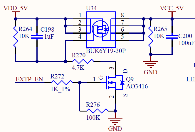
Figure 2
3. Pin Number (5), Signal Name (STANDBY) Design Requirements
It can be used to control the power supply of specific circuits on the carrier board to implement low-power mode in specific scenarios. It controls the conduction of a MOSFET, and a pull-down resistor is designed to ensure an inactive state by default (i.e., the MOSFET is turned ON and power is supplied). When specific scenarios occur, the SoM controls the output high to turn OFF the power to certain circuits on the carrier board. An RC soft-start circuit is required.
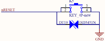
4. Pin Number (6), Signal Name (nRESET) Design Requirements
It is required not to be connected to any pull-up resistor in the design of the carrier board. The high level state is provided by the SoM. The carrier board is connected to a switch button to achieve low level triggering. The debounce capacitor and TVS tube can be reserved according to the situation.
Diagram:
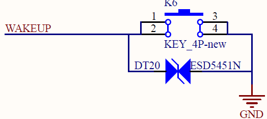
5. Pin Number (7), Signal Name (WAKEUP) Design Requirements
It is required not to be connected to any pull-up resistor in the design of the carrier board. The high level state is provided by the SoM. The carrier board is connected to a switch button to achieve low level triggering. The debounce capacitor and TVS tube can be reserved according to the situation.
Diagram:
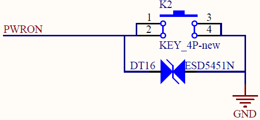
6. Pin Number (8), Signal Name (PWRON) Design Requirements
It is required not to be connected to any pull-up resistor in the design of the carrier board. The high level state is provided by the SoM. The carrier board is connected to a switch button to achieve low level triggering. The debounce capacitor and TVS tube can be reserved according to the situation.
Diagram:
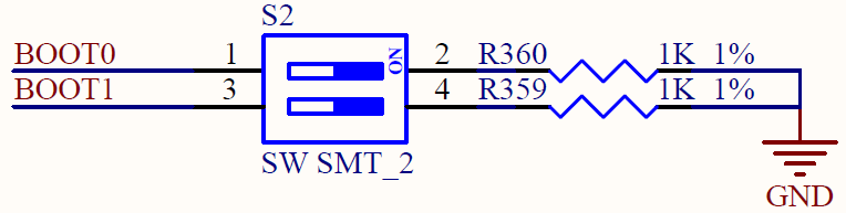
7. Pin Numbers (9/10), Signal Names (BOOT1/BOOT2) Design Requirements
In carrier board design, the two BOOT pins are pulled down to ground through a 1K resistor via a dual-position DIP switch. Pull-up resistors or other circuits are not allowed. Switch configurations as follows:
BOOT MOD |
BOOT1 |
BOOT0 |
|---|---|---|
EMMC |
OFF |
OFF |
TF |
OFF |
ON |
NOR |
ON |
OFF |
NAND |
ON |
ON |
Diagram:
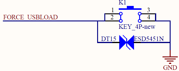
8. Pin Number (11), Signal Name (FORCE_USBLOAD) Design Requirements
It is required not to be connected to any pull-up resistor in the design of the carrier board. The high level state is provided by the SoM. The carrier board is connected to a switch button to achieve low level triggering. The debounce capacitor and TVS tube can be reserved according to the situation.
Diagram:
9. Pin Number (12), Signal Name (POR_B) Design Requirements
It is used to reset the CPU and should only be used in conjunction with the JTAG interface for CPU debugging.
10. Pin Number(34/35/69/70/325/326)Signal Name(I2C)Design Requirements
When designing this pin, it’s essential to add pull-up resistors to the carrier board. Additionally, a 0Ω resistor should be placed before each connected chip to facilitate debugging. If this I2C bus is shared with the SoM, it’s advisable to minimize or avoid using this I2C bus in the carrier board design as much as possible. If you do use it, ensure that there are no address conflicts with the SoM. Furthermore, the hardware manual for this platform specifies the addresses of devices connected to the SoM, the appropriate values for the pull-up resistors, and which other functions cannot be reused.
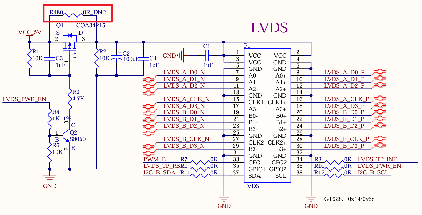
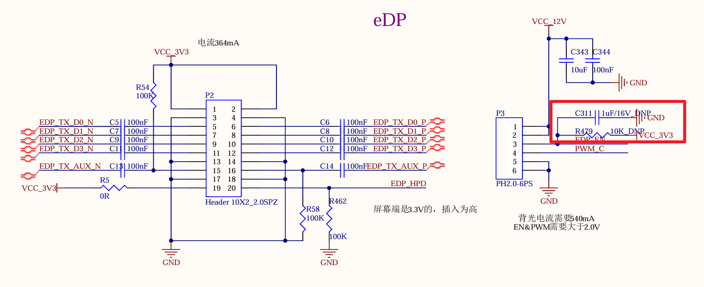
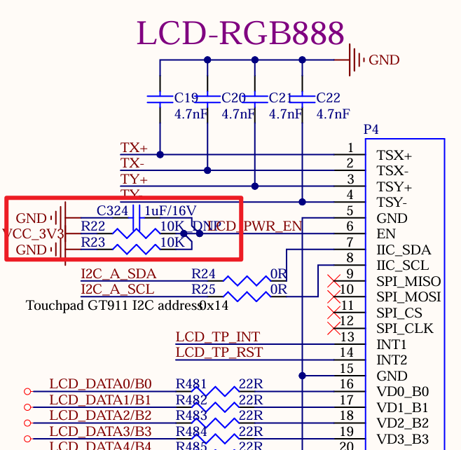
11. Display Interface (LCD/LVDS/MIPI_DSI/HDMI/EDP) Design Requirements
Pin Numbers (191/163/164/358/175/359/371/370), Signal Names (LCD_PWR_EN/PWM_B/LVDS_PWR_EN/PWM_A/EDP_PWR_EN/PWM_C/MIPI_PWR_EN/PWM_D): In carrier board design, it is essential to connect the pins to their respective display interfaces according to their classifications. Each pin requires a pull-down resistor to ensure that it defaults to a low level during power-on, allowing it to be pulled high under SoM control. This setup helps prevent screen flickering during power-up. If an enable (EN) signal is not present, the corresponding display interface should be directly pulled up. Additionally, PWM signals must also have pull-down resistors to avoid flickering of the screen at power-on.
Pin Numbers (271/272/364/365/274/275/178/179/361/362), Pin Names (EDP_TX_AUX/EDP_TX_D0/EDP_TX_D1/EDP_TX_D2/EDP_TX_D3): In carrier board design, it is essential to add DC-blocking capacitors. For the AUX pair, reserve a P-side pull-down and an N-side pull-up resistor.
12. Ethernet Interface (RGMII/RMII) Design Requirements
Pin numbers (284 and 215) and pin names (RGMII_A_RST and RGMII_B_RST) should be connected to the chip’s reset pin through a series resistor. Additionally, an RC circuit must be included to ensure that the PHY resets correctly, even when this signal is not present on the System on Module (SoM).
Pin Numbers (86/87/103/104), Pin Names (RGMII_A_MDIO/RGMII_A_MDC/RGMII_B_MDIO/RGMII_B_MDC): Series resistors are required, and pull-up resistors must be added (the pull-up on the clock line can be left unpopulated).
All signal pins need to be connected to the PHY via series resistors for future debugging purposes.
13. SD Card Interface Design Requirements
When all signals are connected to the SD card and TF card slots, series resistors need to be added and placed close to the stamp holes for debugging purposes. Power should be supplied using the SoM pin number (118) and pin name (SD_A_PWR), with filtering capacitors connected near the slot. Please don’t use carrier board power supply.
14. SDIO Interface Design Requirements
All signal pins need to be connected to the WIFI via series resistors for future debugging purposes. The two signals, BT_HOST_WAKE_B and WIFI_HOST_WAKE_B, must use the dedicated pins on the SoM to ensure the sleep/wake-up functionality. Other control signals can use regular GPIOs.
15. PCIe Interface Design Requirements
All TX signal pins should have series capacitors added on the carrier board connecting to the PCIe slot. All RX signal pins should have series resistors added on the carrier board connecting to the PCIe slot. The clock signals for Group A can be provided either by the carrier board or the SoM to ensure support for both RC and EP modes. The clock signal pins for Group B should have series resistors added on the carrier board connecting to the PCIe slot.
16. USB Interface Design Requirements
Pin Numbers (298/295), Pin Names (USB2_A_VBUS/USB2_B_VBUS): In carrier board design, the 5V power supply must be connected to these pins. In HOST mode, power is supplied by the carrier board; in DEVICE mode, power is supplied by the socket. A power switching control circuit is required.
Pin Numbers (299/296), Pin Names (USB2_A_ID/USB2_B_ID): In carrier board design, only the pull-down function should be retained; do not add pull-ups. The high-level state is provided by the SoM.
For signal pins: USB 2.0 signals must have series resistors reserved when connecting to the socket. For USB 3.0, TX signals require DC-blocking capacitors (series caps), and RX signals require reserved series resistors when connecting to the socket.
17. JTAG Interface Design Requirements
All data pins must have reserved pull-up resistors. The pull-up voltage must match the VREF of the JTAG interface.
1.2 UP4 Platform Carrier Board Schematic Compatibility Design Guide
The UP4 platform is currently compatible with five platforms: RK3568, RK3562, T527, T536, and MX9352. Since the interfaces vary across these platforms, any compatibility design must include redundancy to support switching between them.
1. Reserved Design for Display Interfaces
The UP4 definition supports five display interfaces: LVDS, LCD, MIPI_DSI, HDMI, and eDP. For the enable pins of these display interfaces, it is necessary to reserve RC or series resistors. This ensures that the screen can be enabled normally on platforms where extra I/O pins are unavailable.
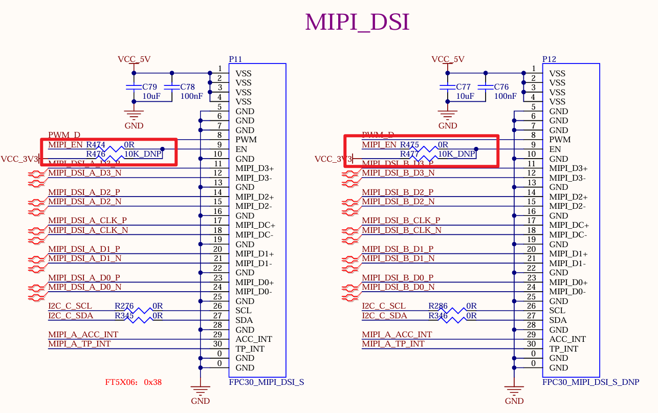
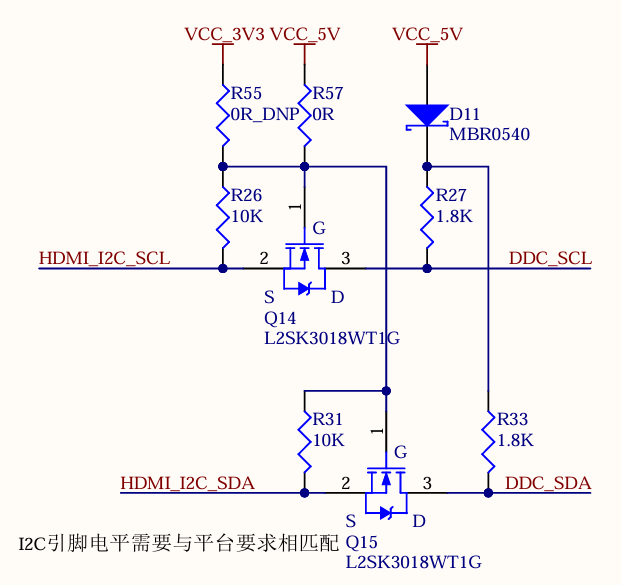
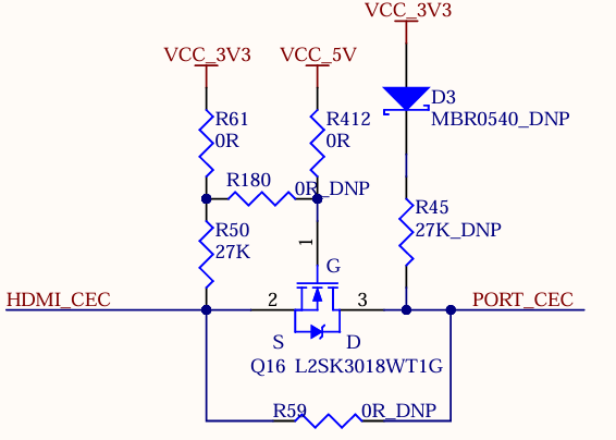
For I2C and CEC of HDMI interface, 3.3 V or 5V level compatibility shall be reserved
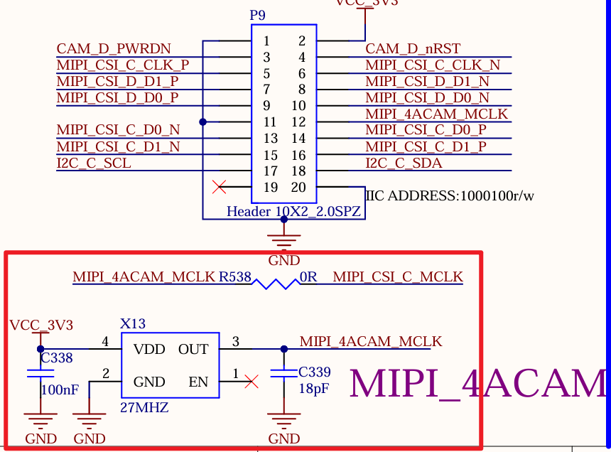
2. Camera Module Design
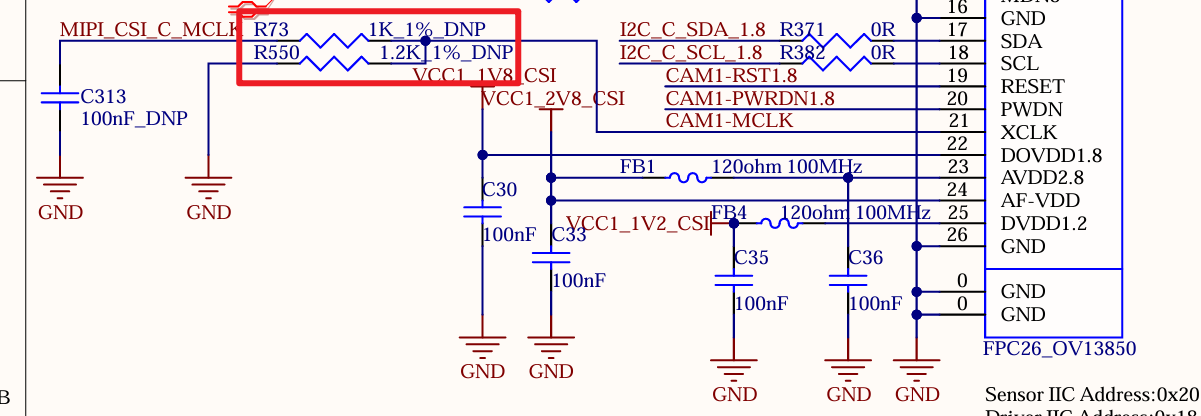
If the Master Clock (MCLK) output from the SoM is required, the series resistors and voltage divider resistors should be reserved in the design to ensure the clock signal level meets the camera module’s requirements.
For four analog camera modules, 27 M active clock shall be reserved to provide clock source for the module when the SoM has no MCLK resource.
3. WiFi Module Design
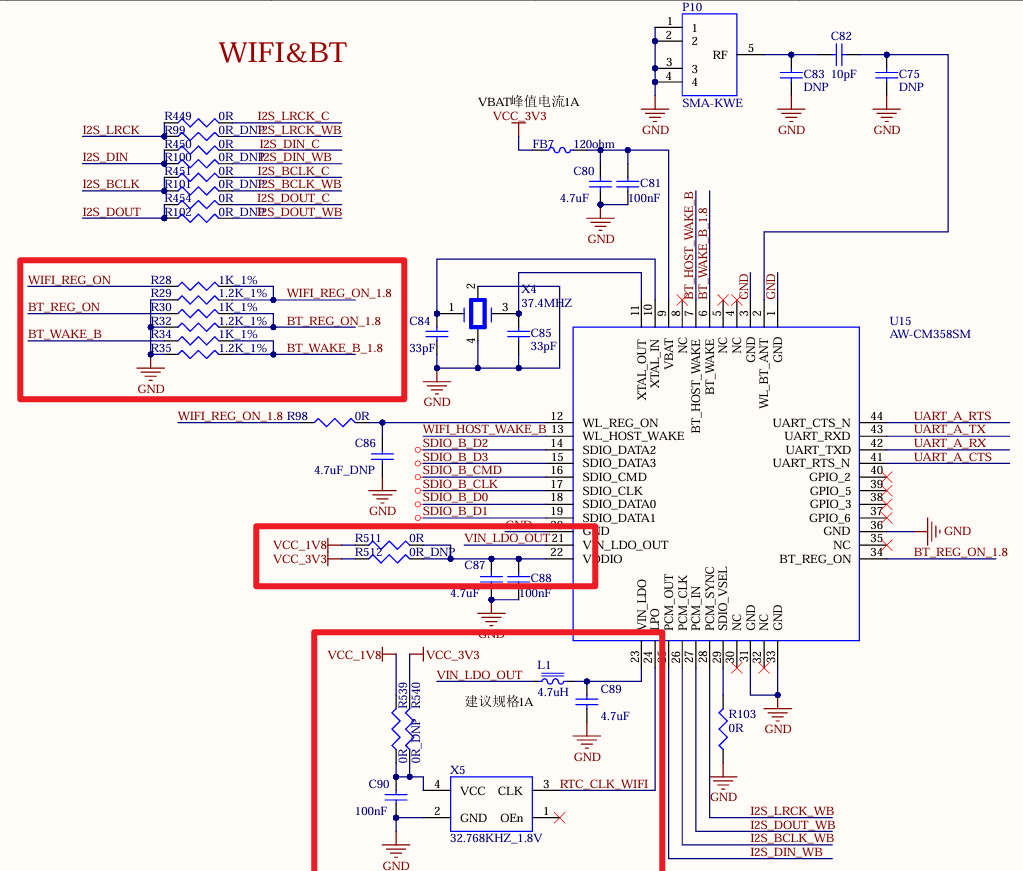
To be compatible with different I/O levels, both 3.3V and 1.8V power supplies should be reserved, and they should also be reserved for the crystal oscillator. The appropriate active crystal oscillator should be selected based on the actual voltage used. Furthermore, a divider resistor should also be reserved for the signal control to match the level.
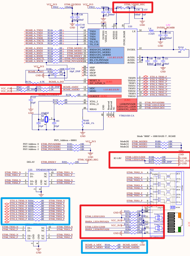
4. Gigabit Ethernet Port Design
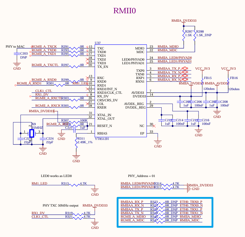
The IO level of 3.3 V and 1.8 V shall be considered, and the level selection option, pull-up level option, and network port status light option shall be reserved. To be compatible with RMII interface, RMII chip shall be designed, and the signal line shall be selectively soldered through the resistor.
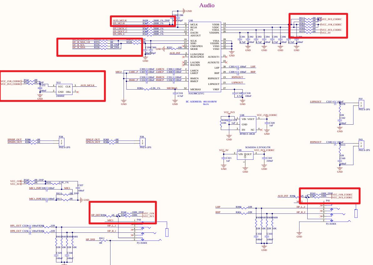
5. Audio Codec Design
To ensure compatibility with 1.8V and 3.3V I/O levels, both 3.3V and 1.8V I/O power supplies should be reserved. The signal pins should also be configured to support both I/O states, selectable via series resistors. Additionally, a 24M active clock should be reserved for the MCLK signal to accommodate platforms without built-in MCLK.
In the PCB BOM, for the USB port, the dual-layer USB socket or single-layer USB socket can be selected for soldering through package compatibility.
2. PCB Design
2.1 PCB Compatibility Design Examples
1. Ethernet Port Compatibility Design Example
2.2 U40 Carrier Board PCB Layout Design Guidelines
This specification can be applied to different PCB designs. You can refer to it and make optimization based on your actual use.
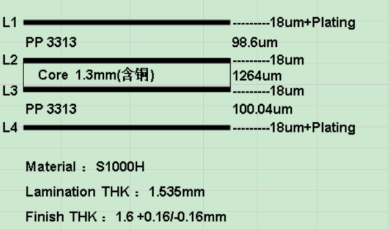
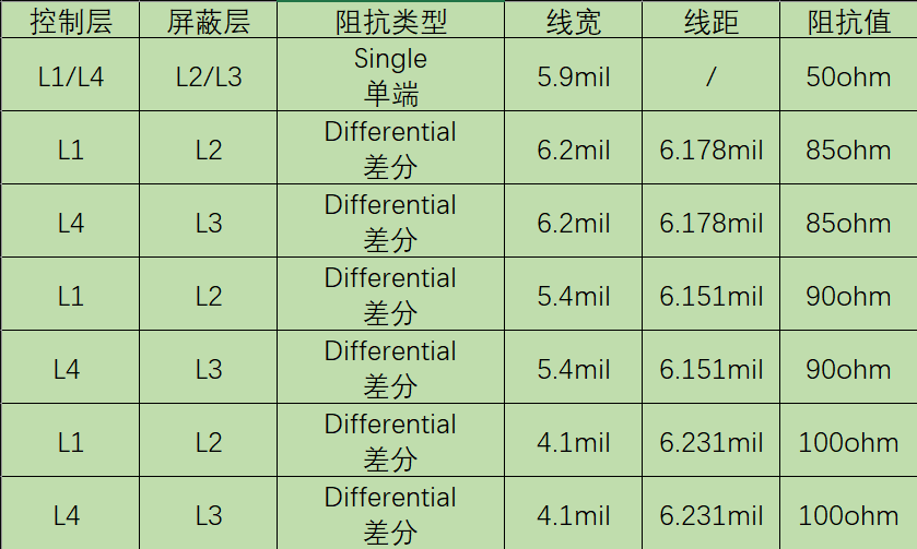
1. Stack-up Configuration
For 4-layer boards, the recommended stack-up is: S1 - POWER - GND - S2. The impedance profile is as shown below:
For 6-layer boards, the recommended stack-up is: S1 - GND - S2 - S3 - POWER - S4. The impedance profile is as shown below:
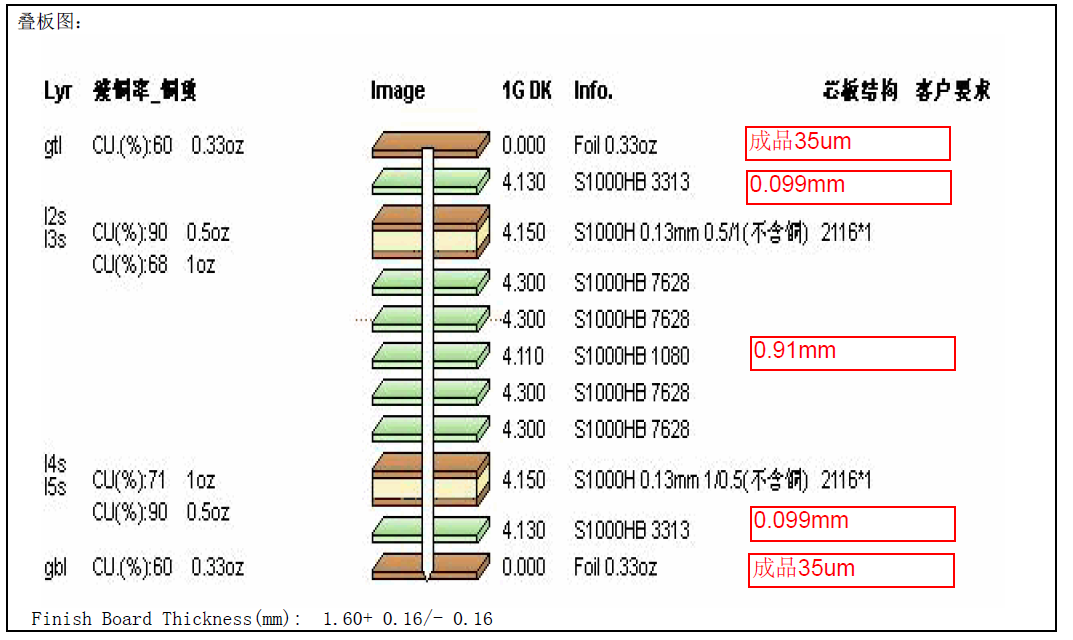
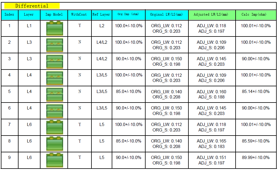
The specific stack-up can be adjusted according to actual requirements.
2. Via Configuration
The preferred via size series:
Hole Size 24mil 20mil 16mil 12mil 8mil Pad Diameter: 40mil 35mil 28mil 25mil 20mil
For the LGA fanout, a 12/20 mil via configuration is recommended.
3. Routing Layout
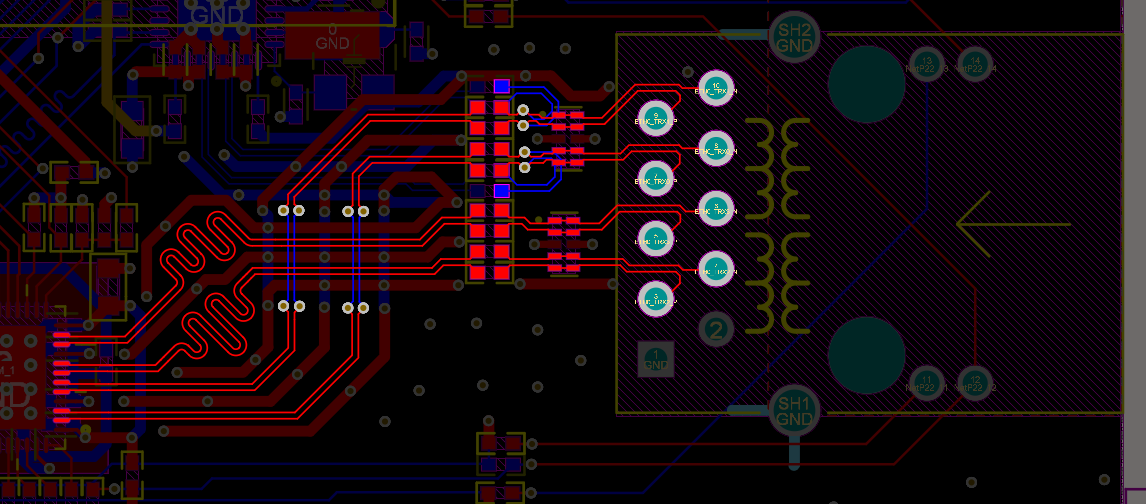
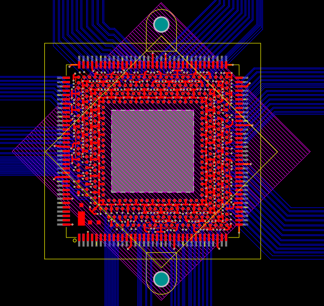
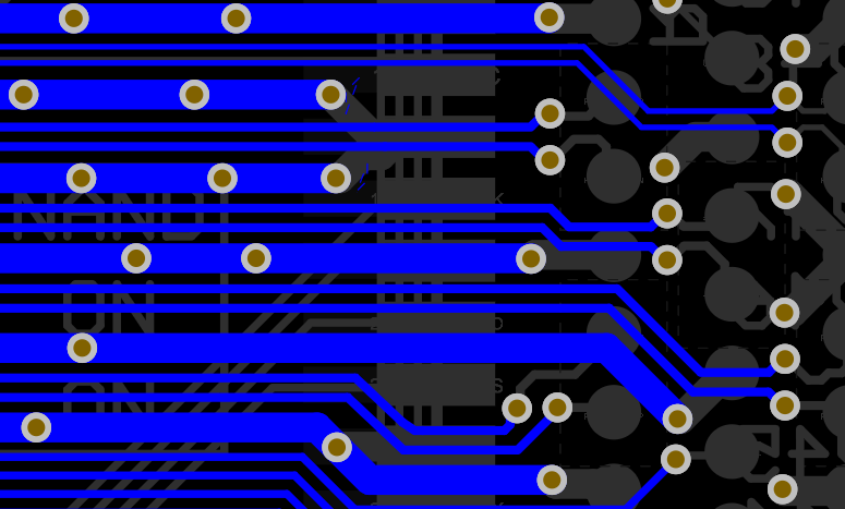
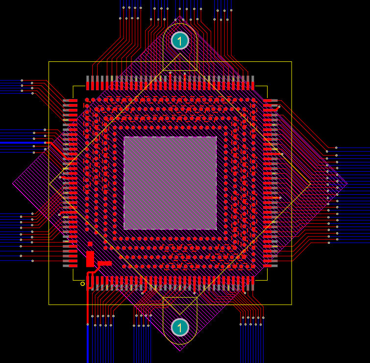
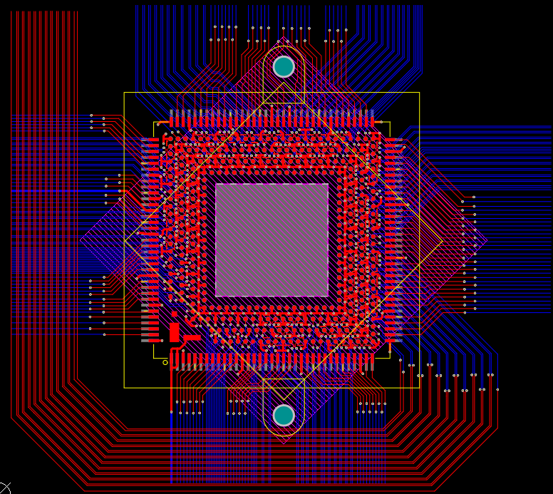
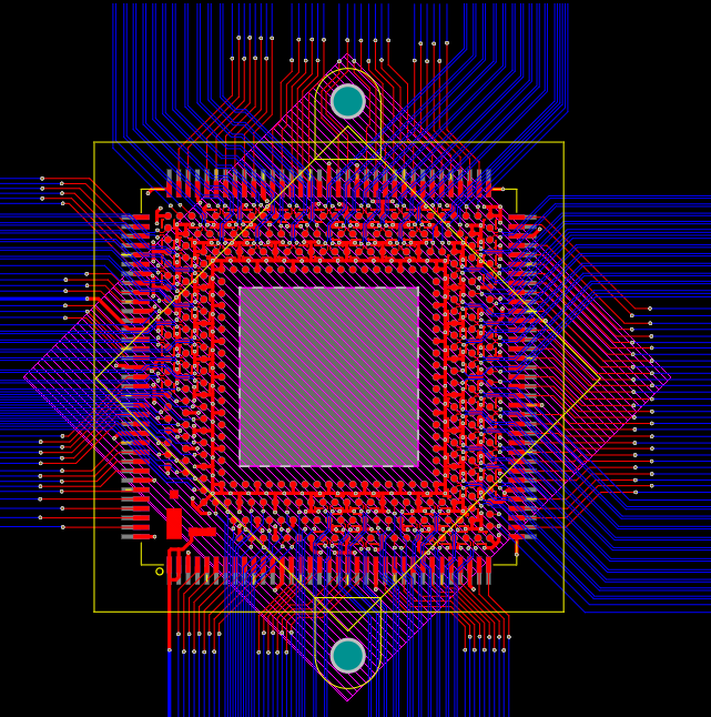
Since the SoM predominantly uses LGA pins, and all differential pairs, along with most high-speed signals, are located in the LGA area, signals from the LGA should be fanned out collectively and routed primarily on the bottom layer to ensure signal integrity. As shown in the figure below:
The fan-out method for LGA differential pairs is illustrated below:
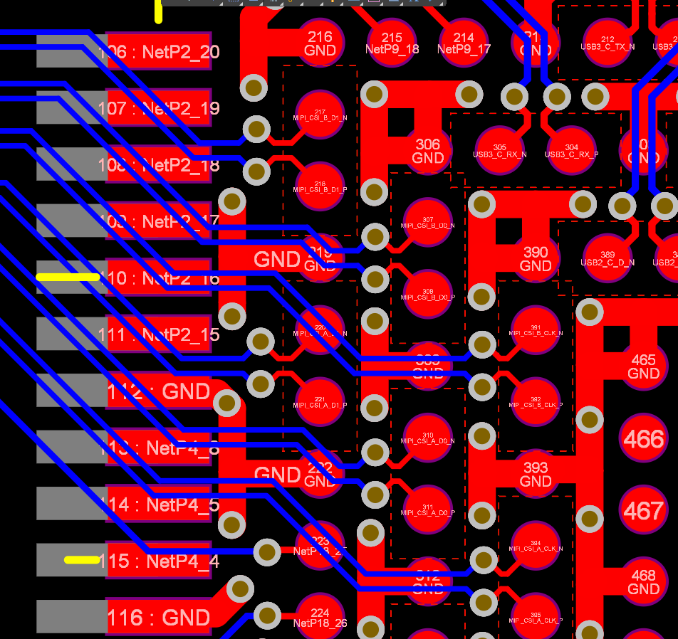
A minimum safety spacing of three times the trace width (3W) should be maintained between differential pairs to prevent signal crosstalk. If conditions permit, it is recommended to implement ground isolation around the differential pairs, as shown in the figure below.
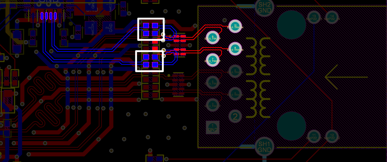
For the LGA differential line pad area on the carrier board, the first two reference layers of the carrier board need to be partially voided to ensure impedance continuity. Please refer to the figure below for the specific voiding area.
For the stamp hole, after completing the normal routing on the top layer, the traces are switched to the bottom layer to ensure that the entire group can be collectively rerouted after exiting.
Schematic of the direction change:
Single-ended 50-ohm impedance traces must maintain at least 2.5W clearance to prevent crosstalk.
The overall routing is as follows:
4. Stencil and Component Placement Requirements
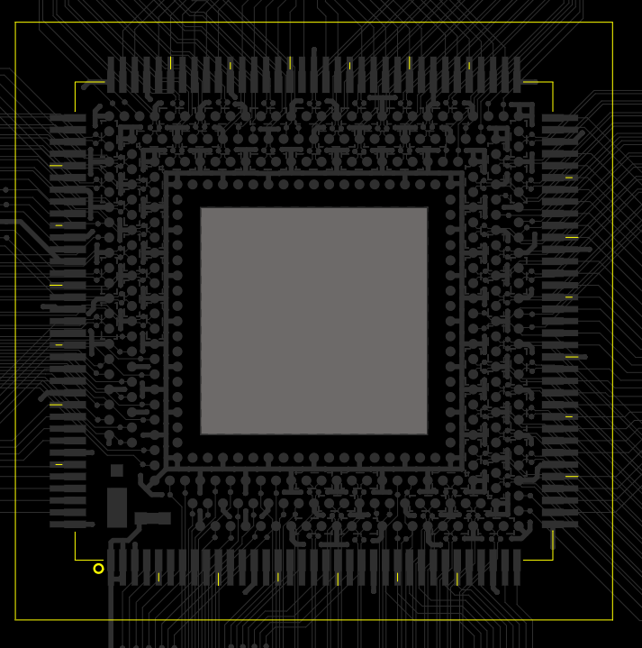
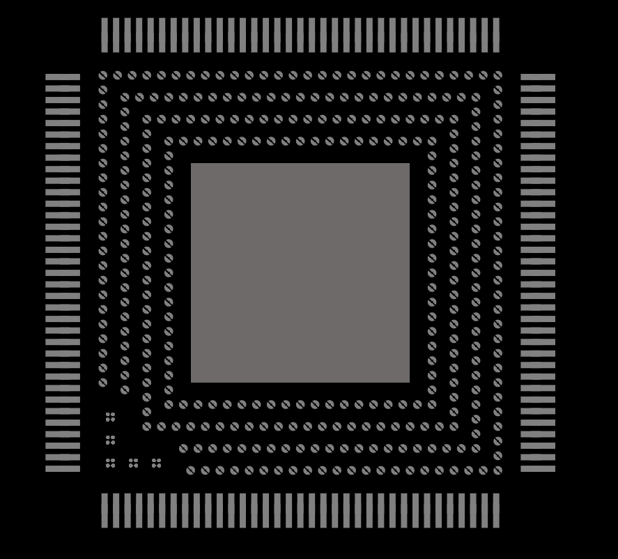
The stencil layer for carrier board footprints is custom-designed. Don’t do modifications to the stencil layer design. The stencil is expanded in the stamp-hole areas. No vias are allowed within these stencil expansion zones. The stencil design is shown below:
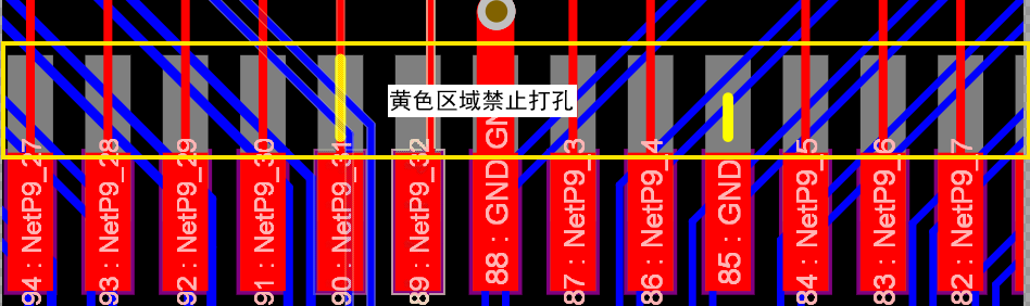
No components shall be placed within 5 mm of the board edge (outside the outer yellow frame in the diagram below). This area is reserved for the stencil used during the separate soldering process of the SoM. This keep-out area may be modified based on practical use.