User’s Hardware Manual_V1.0
Document classification: □ Top secret □ Secret □ Internal information ■ Open
Copyright
The copyright of this manual belongs to Baoding Folinx Embedded Technology Co., Ltd. Without the written permission of our company, no organizations or individuals have the right to copy, distribute, or reproduce any part of this manual in any form, and violators will be held legally responsible.
Forlinx adheres to copyrights of all graphics and texts used in all publications in original or license-free forms.
The drivers and utilities used for the components are subject to the copyrights of the respective manufacturers. The license conditions of the respective manufacturer are to be adhered to. Related license expenses for the operating system and applications should be calculated/declared separately by the related party or its representatives.
Overview
This manual aims to help you quickly get familiar with the product, understand interface functions and configurations. It covers the interface functions and introductions of the development board, product power consumption, and methods for troubleshooting issues during use. Some commands are annotated in the description for user convenience, with a focus on practicality. For information on pin function multiplexing and hardware design guidelines, please refer to Forlinx’s “OK527-UP4 Pin Multiplexing Comparison Table”.
There are four main chapters:
Chapter 1. provides an overall overview of the CPU, briefly introducing its performance and application industries;
Chapter 2. offers a general introduction to the SoM, including descriptions and functions of connector pins;
Chapter 3. introduces the development board in multiple chapters, covering hardware principles and simple design ideas;
Chapter 4. describes the product’s power consumption and other considerations.
Additionally, the manual includes explanations of some symbols and formats.
Format |
Meaning |
|---|---|
Note |
Note or particularly important information must be read carefully. |
📚 |
Relevant explanations regarding the testing section |
️🛤️ |
Related paths. |
Application Scope
This hardware manual applies to Forlinx OK527-UP4, OK527N-UP4 development board (version 1.3 and above) and FET527-UP4, FET527-UP4 SoM (version 1.2 and above). In the manual, the product is referred to collectively as FET527-UP4 or OK527-UP4.
Revision History
Date |
Version |
SoM Version |
Carrier Board Version |
Revision History |
|---|---|---|---|---|
02/03/2026 |
V1.0 |
V1.2 |
V1.3 and above |
Initial Version |
13/05/2026 |
V1.1 |
V1.2 |
V1.3 and above |
1. Removing the pre-tinning information for the SoM. |
1. Allwinner T527 Description
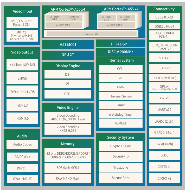
T527 series features a high-performance octa-core Cortex-A55 AI platform SoC, suitable for commercial, industrial, and automotive applications. It integrates an octa-core Cortex-A55 CPU, a HiFi4 DSP, a 2 TOPS NPU, and a G57 MC1 GPU, supporting 4K@30fps H.265 decoder, 4K@30fps H.264 encoder, 1080p@60fps H.264 encoder, along with DI and SmartColor systems, delivering smooth performance and professional AI visual effects.
Applications:
Commercial displays / Point of Sale systems
Cloud PCs
Robotics
Industrial intelligence
Edge computing gateways
Aftermarket infotainment systems
Commercial vehicles
Industrial PC
……
T527 Block Diagram
2. FET527-UP4 SoM Description
2.1 FET527-UP4 Appearance Diagram
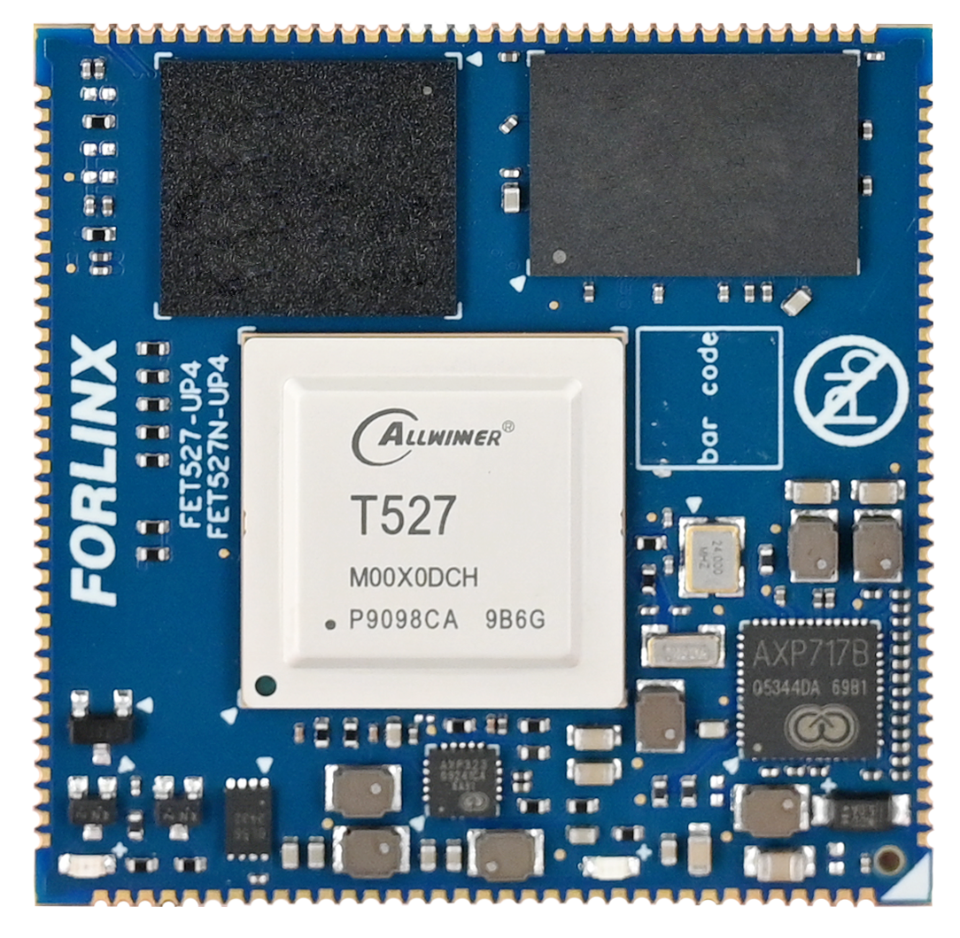
Front
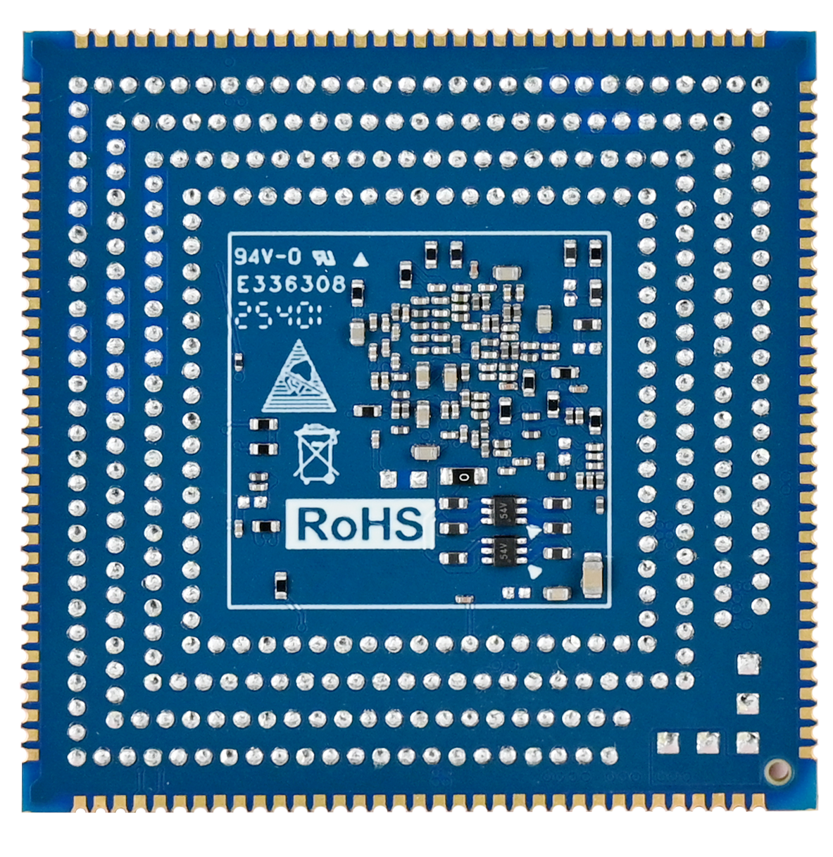
Back
2.2 FET527-UP4 SoM Dimension Diagram
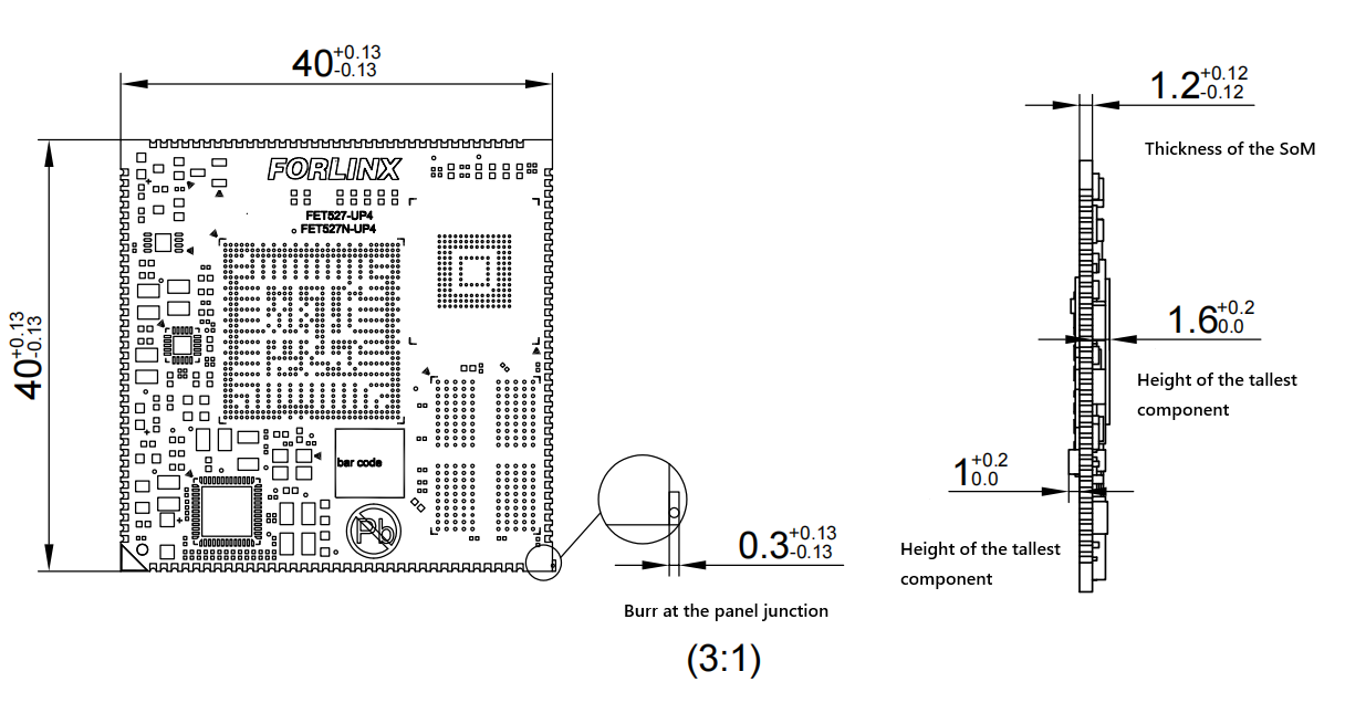
Dimensions: 40mm × 40mm, dimensional tolerance ±0.13mm. For more dimensional details, please refer to the DXF file.
Plate making process: 1.6mm thickness, 10-layer immersion gold PCB.
2.3 Performance Parameter
2.3.1 System Frequency
Name |
Specification |
Description |
|||
|---|---|---|---|---|---|
Minimum |
Typical |
Maximum |
Unit |
||
System Frequency |
— |
— |
1.8 |
GHz |
— |
System RTC |
— |
32.768 |
— |
KHz |
— |
2.3.2 Power Parameter
Parameter |
Pin No. |
Specification |
Description |
|||
|---|---|---|---|---|---|---|
Minimum |
Typical |
Maximum |
Unit |
|||
Main Power Voltage |
VSYS |
3.9 |
5 |
5.25 |
V |
— |
No-load current |
— |
mA |
Please refer to the power consumption table in the appendix |
|||
Overload current |
— |
mA |
Please refer to the power consumption table in the appendix |
2.3.3 Working Environment
Parameter |
Specification |
Description |
||||
|---|---|---|---|---|---|---|
Minimum |
Typical |
Maximum |
Unit |
|||
Operating Temperature |
Working Environment |
0 |
25 |
+70 |
℃ |
Commercial Level |
Storage Environment |
-40 |
25 |
+125 |
℃ |
||
Working Environment |
-40 |
25 |
+85 |
℃ |
Industrial Level |
|
Storage Environment |
-40 |
25 |
+125 |
℃ |
||
Humidity |
Working Environment |
10 |
— |
90 |
%RH |
No Condensation |
Storage Environment |
5 |
— |
95 |
%RH |
2.3.4 ESD Features
Parameter |
Specification |
Unit |
Description |
|
|---|---|---|---|---|
Minimum |
Maximum |
|||
ESD HBM(ESDA/JEDEC JS-001-2017) |
-2000 |
+2000 |
V |
Applicable to all pins of the SoM |
ESD CDM(ESDA/JEDEC JS-002-2018) |
-250 |
+250 |
V |
Applicable to all pins of the SoM |
Note:
The above data is from the chip manual;
All signal led out from the SoM are electrostatic discharge (ESD) sensitive. When designing carrier board, adequate ESD protection measures must be implemented for the interfaces. Additionally, proper ESD precautions should be observed during the transportation, assembly, and usage of the SoM.
2.4 Interface Resources
2.4.1 FET527-UP4 SoM Interfaces
Function |
Quantity |
Parameter |
|---|---|---|
MIPI CSI |
3 |
8M@30fps RAW12 2F-WDR, maximum size 3264(H) x 2448(V), supported lane configurations 4+2+2-lane |
MIPI DSI |
1 |
Supports 4-lane MIPI DSI, 1280 x 720@60fps and 1920 x 1200@60fps |
LVDS |
1 |
Supports dual link 1920 x 1080@60fps, single link 1366 x 768@60fps; |
eDP1.3 |
1 |
Supports 2.5K @ 60 fps and 4K @ 30 fps; |
HDMI2.0 |
1 |
Supports 2D display at 4K @ 60 fps, 3D display at 4K @ 30 fps; |
Audio Codec |
1 |
One stereo headphone output; two differential LINEOUT outputs; one differential MIC input. |
I2S |
1 |
Sampling rates range from 8 kHz to 384 kHz |
CAN |
2 |
The baud rate is up to 1Mbps |
USB |
3 |
1×USB3.0, supporting OTG; |
SDIO |
2 |
SDC0: for SD card, up to 200 MHz in SDR mode |
SPI |
2 |
SPI2: Supports SPI master/slave mode, up to 100 MHz; |
UART |
3 |
Compatible with industry standards 16450/16550 |
GMAC |
2 |
Support RMII/RGMII interface and rate 10/100/1000 Mbit/s |
GPADC |
3 |
12-bit sampling resolution and 10-bit accuracy, maximum sampling rate 1MHz |
LRADC |
1 |
6-bit sampling resolution with a 2 kHz sampling rate for key detection. |
PWM |
3 |
Output frequency 024MHz or 0100MHz |
I2C |
3 |
Standard mode 100 kbit/s, fast mode 400 kbit/s |
2.4.2 CPU Interfaces
Function |
Quantity |
Parameter |
|---|---|---|
Parallel CSI |
1 |
Supports 8/10/12/16-bit widths; ITU-R BT.656 up to 4_720P@30fps, and ITU-R BT.1120 up to 4_1080P@30fps |
MIPI CSI |
≤4 |
8M@30fps RAW12 2F-WDR, maximum size 3264(H) x 2448(V), supported lane configurations 4+4-lane, 4+2+2-lane, or 2+2+2+2-lane |
MIPI DSI |
≤2 |
Supports 4-lane MIPI DSI, 1280 x 720@60fps and 1920 x 1200@60fps; |
RGB |
≤2 |
TCON_LCD0 supports DE/SYNC mode, 1920 x 1080@60fps; |
LVDS |
≤2 |
Supports dual link 1920 x 1080@60fps, single link 1366 x 768@60fps; |
eDP1.3 |
1 |
Supports 2.5K @ 60 fps and 4K @ 30 fps; |
HDMI2.0 |
1 |
Supports 2D display at 4K @ 60 fps, 3D display at 4K @ 30 fps; |
Audio Codec |
1 |
One stereo headphone output; two differential LINEOUT outputs; three differential MIC inputs. |
I2S/PCM |
≤4 |
Sampling rates range from 8 kHz to 384 kHz |
DMIC |
1 |
Supports 8-channel with sampling rate from 8kHz to 48kHz |
OWA IN/OUT |
1 |
Single-wire audio |
CAN |
≤2 |
The baud rate is up to 1Mbps. |
USB |
≤3 |
USB0: USB2.0 OTG, 480Mbps |
PCIe2.1 |
1 |
RC mode only, 1-lane, 5Gbps |
SDIO |
≤2 |
SDC0: for SD card, up to 200 MHz in SDR mode |
SPI |
≤4 |
SPI0: Supports SPI master/slave mode, up to 100 MHz; |
TWI |
≤8 |
Compatible with I2C standard, standard mode 100 kbit/s, fast mode 400 kbit/s |
UART |
≤10 |
Compatible with industry standards 16450/16550 |
GMAC |
≤2 |
Support RMII/RGMII interface and rate 10/100/1000 Mbit/s |
GPADC |
14 |
12-bit sampling resolution and 10-bit accuracy, maximum sampling rate 1MHz |
LRADC |
2 |
6-bit sampling resolution with a 2 kHz sampling rate for key detection. |
PWM |
≤30 |
Output frequency 024MHz or 0100MHz |
CIR TX/RX |
1 |
Infrared signal sending/receiving |
Note: The parameters in the table are the theoretical values of hardware design or CPU.
2.5 FET527-UP4 SoM Pin Definitions
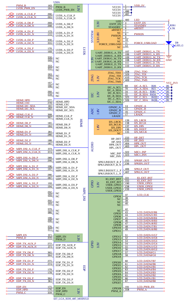
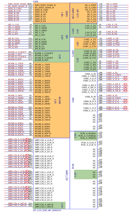
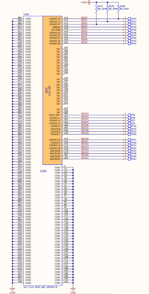
2.5.1 FET527-UP4 SoM Pin Schematic
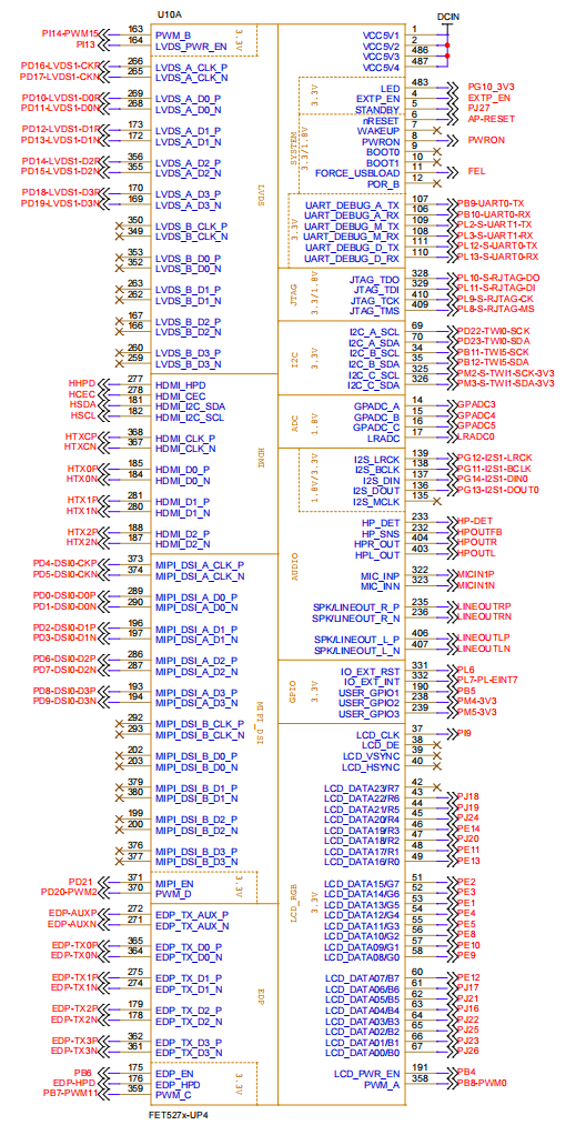
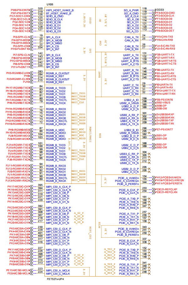
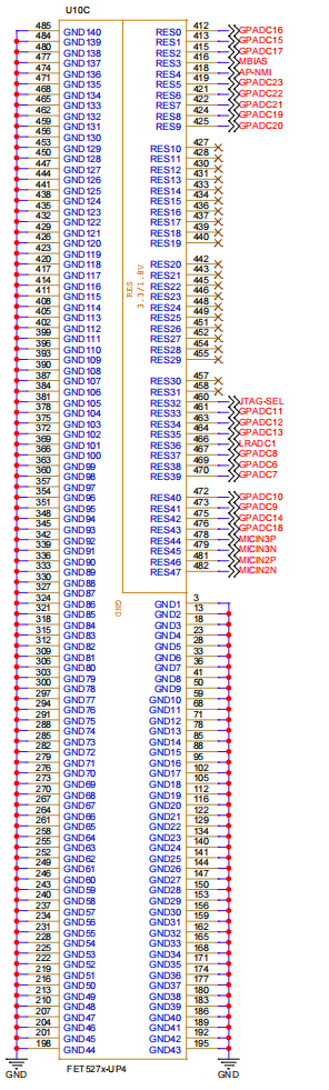
2.5.2 FET527-UP4 SoM Pin Function Description
For various functional expansion requirements, please refer to the user document “FET527-UP4 Pin Multiplexing Table”. However, for more detailed information, it is recommended that you consult the relevant documentation, the chip datasheet, and the reference manual.
2.6 FET527-UP4 SoM Pin Definitions
UP4 Standard Interface Functions |
FET527x-UP4 Pinout Functions |
|---|---|
EXTP_EN |
EXTP_EN |
STANDBY |
PJ27 |
nRESET |
AP-RESET |
WAKEUP |
NC |
PWRON |
PWRON |
BOOT0/BOOT1 |
NC |
FORCE_USBLOAD |
FEL |
POR_B |
NC |
GPADC_A/B/C |
GPADC3/4/5 |
LRADC |
LRADC0 |
SPI_A |
NC |
SPI_B |
NC |
CAN_A |
PI15/16-CAN |
CAN_B |
PL4/5-S-CAN |
UART_A |
PG6/7/8/9-UART1 |
UART_B |
PB0/1/2/3-UART2 |
UART_C |
PI0/1-UART4 |
UART_D |
PB13/17-UART7 |
I2C_A |
PD22/23-TWI0 |
I2C_B |
PB11/12-TWI5 |
I2C_C |
PM2/3-S-TWI1 |
RGMII_A |
RGMII0 |
RGMII_B |
RGMII1 |
RMII_A |
NC |
RMII_B |
NC |
DEBUG_A |
PB9/10-UART0 |
DEBUG_M |
PL2/3-S-UART0 |
DEBUG_D |
PL12/13-S-UART1 |
SD_A |
SDC0 |
SDIO_B |
SDC1 |
I2S |
I2S1 |
Native HP |
NC |
Native SPKOUT_L |
LINEOUTP/LINEOUTN |
Native SPKOUT_R |
NC |
Native MIC |
NC |
PCIE_A |
NC |
PCIE_B |
NC |
LCD |
NC (for GPIO pins) |
MIPI DSI_A |
DSI0 |
MIPI DSI_B |
NC |
LVDS_A |
LVDS1 |
LVDS_B |
NC |
EDP |
NC |
HDMI |
NC |
USB2_A |
USB0 |
USB3_A |
USB0 |
USB2_B |
USB1 |
USB2_C |
USB2 |
USB3_C |
NC |
USB2_D |
NC |
MIPI CSI_A |
MCSIC |
MIPI CSI_B |
MCSID |
MIPI CSI_C |
MCSIA |
MIPI CSI_D |
MCSIB |
JTAG |
RJTAG |
USER_GPIO1 |
PB5 |
USER_GPIO2 |
PM4 |
USER_GPIO3 |
PM5 |
RES0 |
GPADC16 |
RES1 |
GPADC15 |
RES2 |
GPADC17 |
RES3 |
MBIAS |
RES4 |
AP-NMI |
RES5 |
GPADC23 |
RES6 |
GPADC22 |
RES7 |
GPADC21 |
RES8 |
GPADC19 |
RES9 |
GPADC20 |
RES10 |
NC |
RES11 |
NC |
RES12 |
NC |
RES13 |
NC |
RES14 |
NC |
RES15 |
NC |
RES16 |
NC |
RES17 |
NC |
RES18 |
NC |
RES19 |
NC |
RES20 |
NC |
RES21 |
NC |
RES22 |
NC |
RES23 |
NC |
RES24 |
NC |
RES25 |
NC |
RES26 |
NC |
RES27 |
NC |
RES28 |
NC |
RES29 |
NC |
RES30 |
NC |
RES31 |
NC |
RES32 |
JTAG-SEL |
RES33 |
GPADC11 |
RES34 |
GPADC12 |
RES35 |
GPADC13 |
RES36 |
LRADC1 |
RES37 |
GPADC8 |
RES38 |
GPADC6 |
RES39 |
GPADC7 |
RES40 |
GPADC10 |
RES41 |
GPADC9 |
RES42 |
GPADC14 |
RES43 |
GPADC18 |
RES44 |
MICIN3P |
RES45 |
MICIN3N |
RES46 |
MICIN2P |
RES47 |
MICIN2N |
It is the UP4 standard definition. If compatible design is required, it is recommended to design according to it.
2.7 SoM Hardware Design Description
Power Pin
Function |
Signal Name |
I/O |
Default Function |
Pin Number |
|---|---|---|---|---|
Power supply |
VCC5V0_SYS |
Power Input |
Power Supply for SoM: Voltage: 5V |
|
VCC3V3_SD |
Power output |
Only used for power supply of carrier board SD card, |
||
GND |
Ground |
Power ground and signal ground on the SoM. |
System Control Pin
Function |
Signal Name |
I/O |
Default Function |
Pin Number |
|---|---|---|---|---|
CPU reset |
RESETn |
I |
SoM power reset, low level effective. Do not add additional capacitive load to this pin, |
6 |
Power enable |
PMIC_EXT_EN |
O |
Enable signal to control the external power supply of the carrier board, output by the SoM, 3.3 V level. |
4 |
On/Off |
PMIC_PWRON |
I |
Low level is valid, long press to turn off, short press to turn on. |
8 |
BOOT selection |
EMMC_BOOT |
I |
When the signal is grounded, the startup card enters the Maskrom download mode. |
1 |
Wake up |
WAKEUP |
I |
SoM wake-up button |
7 |
Debug Port |
UART2_TX_M0_DEBUG UART2_RX_M0_DEBUG |
I/O |
Debug Port, please keep the port functions. |
106 107 |
(Including minimum system block diagram)
The FET527-UP4 SoM integrates power, reset monitoring, and storage circuits, requiring only minimal external circuitry. A complete minimum system can be powered and run with a single 5V supply.
Refer to “Appendix IV. Minimum System Diagram” However, in most cases, it is recommended to connect some external devices—such as a debugging serial port and a port for flashing images—in addition to the minimal system. Otherwise, you can not check whether the system has booted. After completing these steps, you can then add the required functions based on the SoM’s default interface definition provided by Forlinx.
For the design of the SoM’s peripheral circuits, please refer to Section 3.5, “OK527-UP4 Carrier Board Description”.
3. OK527-UP4 Embedded Development Platform Description
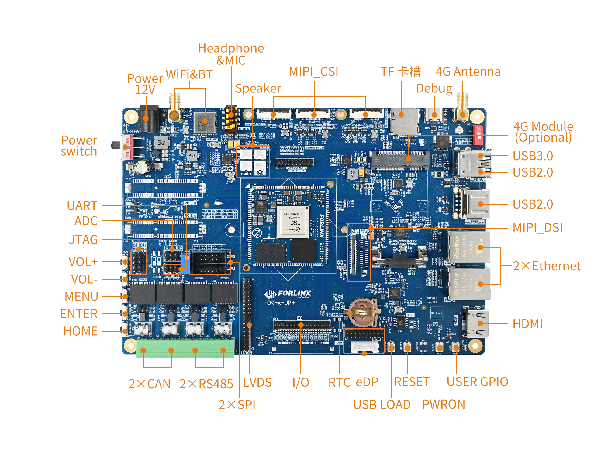
3.1 OK527-UP4 Development Board Interface Diagram
Connection method: Stamp hole + LGA.
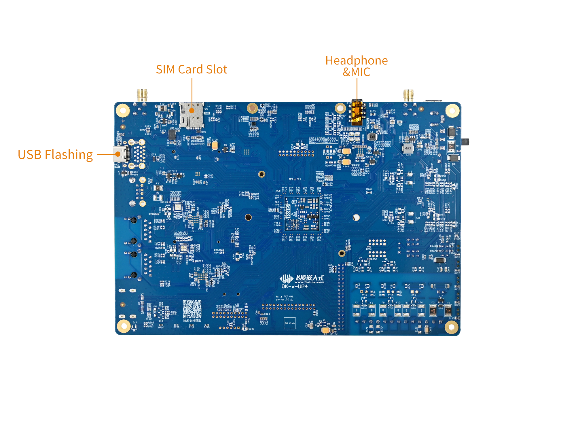
The main interfaces are shown in the figure below:
3.2 OK527-UP4 Development Board Dimension Diagram
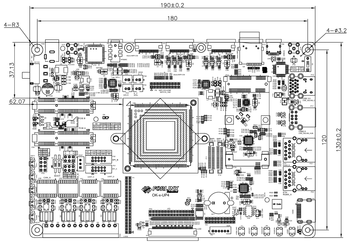
PCB: 130mm×190mm
Mounting hole dimensions: Pitch: 120mm × 180mm, hole diameter: 3.2mm.
Plate making process: 1.6mm thickness, 4-layer PCB.
Power Voltage: DC 12V
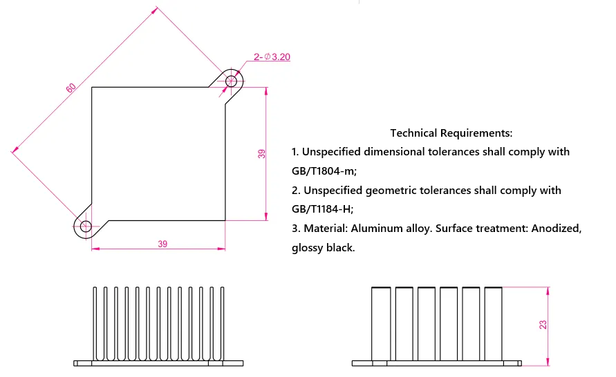
The OK527x-UP4 carrier board is equipped with two mounting holes for heat sinks (3.2 mm in diameter). You may choose to install a heat sink according to the on-site environment. Please add a insulating thermal pad between the contact surface of the heat sink and the SoM. Recommended heat sink: 39mm × 39mm × 23mm. See below for details.
3.3 Naming Rules
A-B-C+D E F :G-H
Field |
Field Description |
Value |
Description |
|---|---|---|---|
A |
Product Line Identification |
OK |
Forlinx Embedded Carrier Boards/Development Boards |
- |
Separator |
- |
|
B |
CPU Name |
527 |
T527 |
- |
Segment Identification |
- |
Parameter separator |
C |
Connection |
UP4 |
Package general package 4 means 40*40 |
+ |
Segment Identification |
+ |
The configuration parameter section follows this identifier. |
D |
Type Label |
M |
Carrier board (Carrier board is marked with M, not filled in by default) |
E |
Operating Temperature |
I |
-40 to 85℃ Industrial-grade |
F |
PCB Version |
13 |
V1.3 |
xx |
Vx.x |
||
: |
Separator |
: |
It is followed by the manufacturer’s internal identification. |
G |
Connector Origin |
N |
No Partition\No Connector |
- |
Hyphen |
- |
Grade Mark Connector |
H |
Grade Identification |
Blank |
Mass Production |
3.4 Carrier Board Interfaces
Function |
Quantity |
Parameter |
|---|---|---|
WiFi |
1 |
Single antenna 2.4G&5GHz |
Bluetooth |
1 |
|
Audio |
2 |
Dual-channel speaker connector, class-D, 1.3 W; |
MIPI-CSI |
3 |
Led out via FPC connector; |
TF Card |
1 |
Data rate up to SDR104; |
4G |
1 |
Supports 4G modules with a miniPCIE interface, integrating USB2.0 communication signals. |
UART Debug |
1 |
Integrated into a single Type-C port, enabling connection to a PC for debugging. |
USB3.0 |
1 |
USB_A can switch between master and slave modes and supports USB flashing; USB_C only supports slave mode. |
USB2.0 |
2 |
One USB_D port (native USB 2.0) and one USB_HUB port |
Ethernet |
2 |
Standard RJ45 socket with two Gigabit ports |
HDMI |
1 |
Supports HDMI 2.1, with a maximum resolution of 4096×2304@60Hz |
EDP |
1 |
Supports eDP 1.3, with a maximum resolution of 2560×1600@60Hz |
MIPI-DSI |
2 |
4-lane MIPI-DSI, supporting capacitive touch screen and backlight brightness adjustment. |
RTC |
1 |
On-board CR1220 battery, keep going when power is off |
LVDS |
1 |
4-lane LVDS, supports capacitive touchscreens, supports backlight brightness adjustment, supports 1280×800@60Hz |
RS485 |
2 |
Electrical quarantine |
CAN |
2 |
Supports CAN2.0B, electrical quarantine |
ADC |
3 |
Led out from the pin header and can be connected to the on-board sliding rheostat. |
SPI |
2 |
2 x SPI led out via a simple terminal block, and can be used to connect peripherals for debugging functionality. |
UART |
1 |
5-wire UART, pin header connection |
JTAG |
1 |
JTAG interface is routed out via pin headers. |
KEY ADC |
5 |
1 x SARADC, five buttons are routed out |
Note: The parameters in the table are the theoretical values of hardware design or CPU.
3.5 OK527-UP4 Carrier Board Description
Note:
The component UID with “_DNP” mark in the diagram below represents it is not soldered by
default;The schematic diagrams in this manual are only for interface descriptions. Please refer to the source file materials for hardware design.
3.5.1 Carrier Board Power
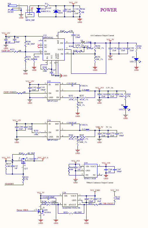
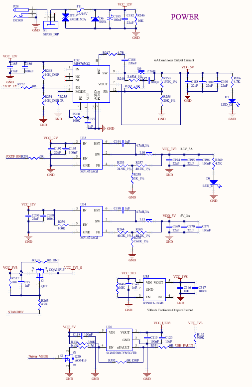
As shown, the power supply for the development board is 12V DC (from P28). VDD_5V supplies power to the SoM. Once the SoM is powered up, it outputs PMIC_EXT_EN to enable U32 and U33 on the carrier board, and VCC_5V, VCC_3V3, and VCC_1V8 supply power to the devices on the carrier board. The STANDBY pin controls VCC_3V3_S to enable or disable the power supply for the development board, achieving reduced power consumption.
PMIC_EXT_EN ensure to power on the SoM first, followed by the carrier board, to prevent latch-up effects that could damage the CPU.
3.5.2 Power/Reset Keys
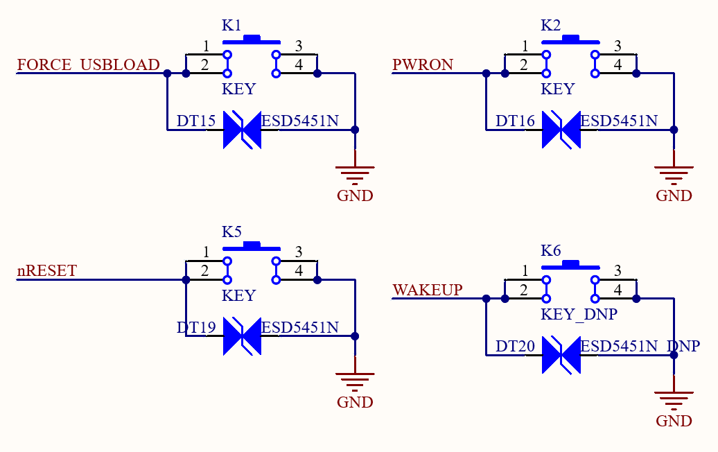
K1 on the carrier for USB programming. Holding K1 before powering on enables USB programming.
K2 on the carrier board is for powering ON/Off. By default, the board runs automatically when powering on. While running, press and hold the key to shut down; press it shortly to restart.
K5 on the carrier board is for the resetting. Press it reset the power on the SoM to achieving a full board power reset.
K6 on the carrier board is for waking up. After the board enters sleep mode press it shortly to wake up the board.
The FET527x-UP4 SoM does not support the WAKEUP function.
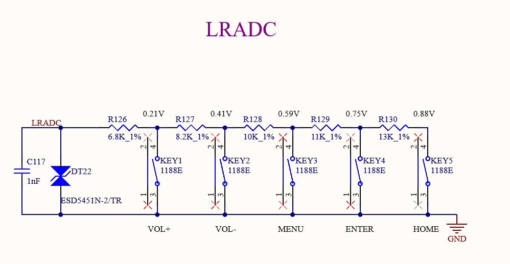
3.5.3 LRADC Button
The carrier board is configured with 1 x LRADC signal, utilizing a button and a resistor voltage divider to enable key value sampling. The LRADC is pulled up to 1.8V via a 10K resistor on the SoM.
3.5.4 Debugging Serial Port
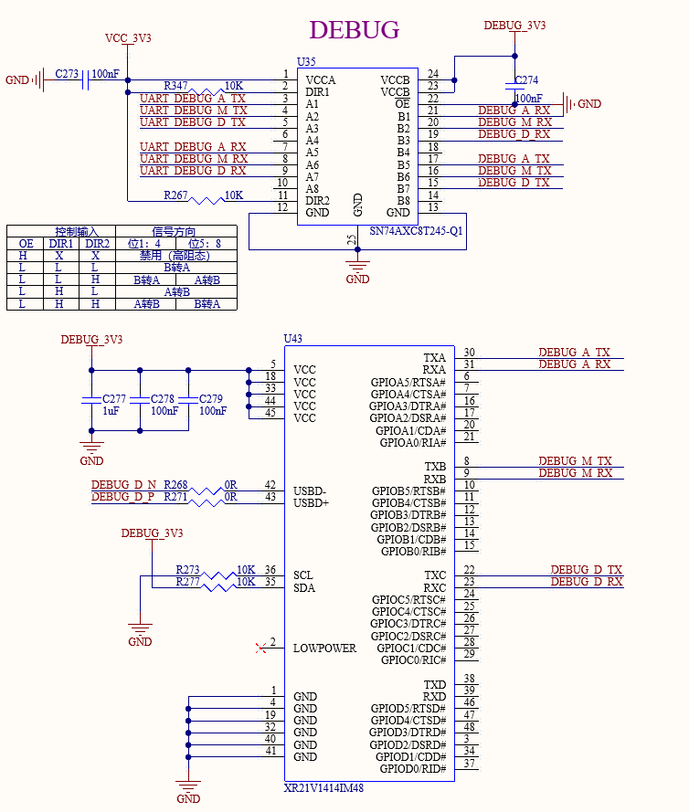
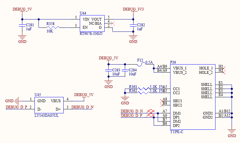
The carrier board features a single USB Type-C port with 3 x integrated debug serial ports. Install the XR21V1414IM48 driver on your computer, connect the P36 port to the computer, and select the DEBUG_A debug serial port to start debugging.
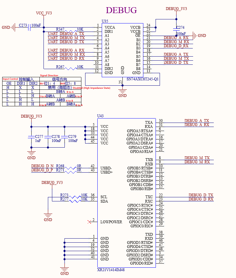
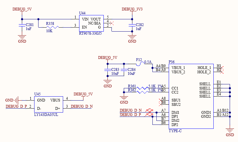
Note: To facilitate debugging later, please ensure that the debugging serial port is led out when designing your own carrier board.
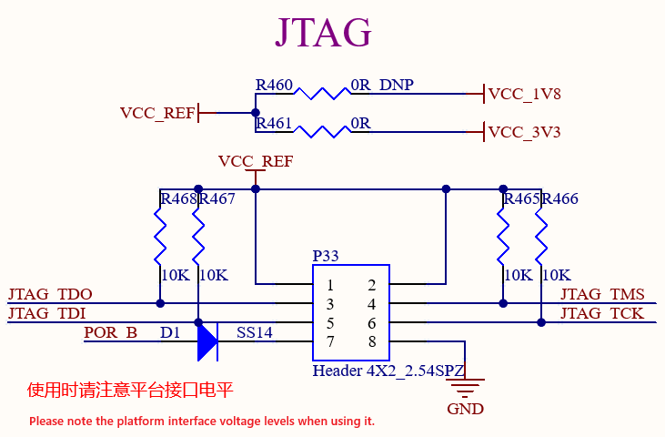
3.5.5 JTAG
The carrier board features a single JTAG debugging interface for debugging the x-core
3.5.6 RTC
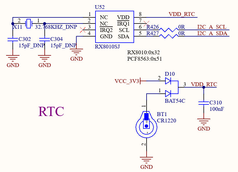
An RTC device is connected to the carrier board via the I2C_A bus. It enables a compatible power supply from either VCC_3V3 or a button cell battery via D10, which ensures the RTC chip remains powered by the battery after the carrier board is powered off. The RX8010SJ chip is used in the default design. Button battery: CR1220.
3.5.7 TF Card
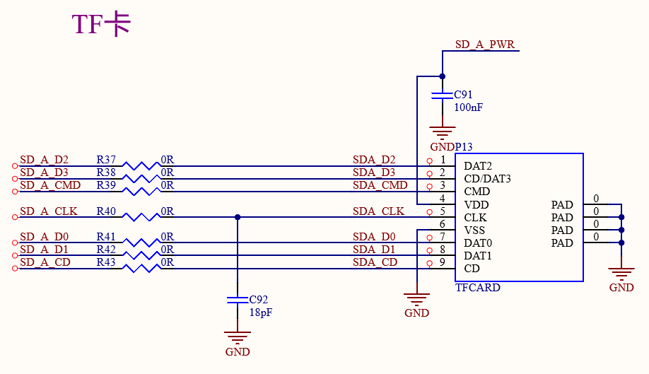
The TF card interface on the development board is connected to the CPU’s SDMMC0 channel. Power for the TF card is supplied by the VCC_3V3_SD output from the SoM
Note:
The bus pull-up resistor has already been configured on the SoM. Don’t apply pull-up to the bus;
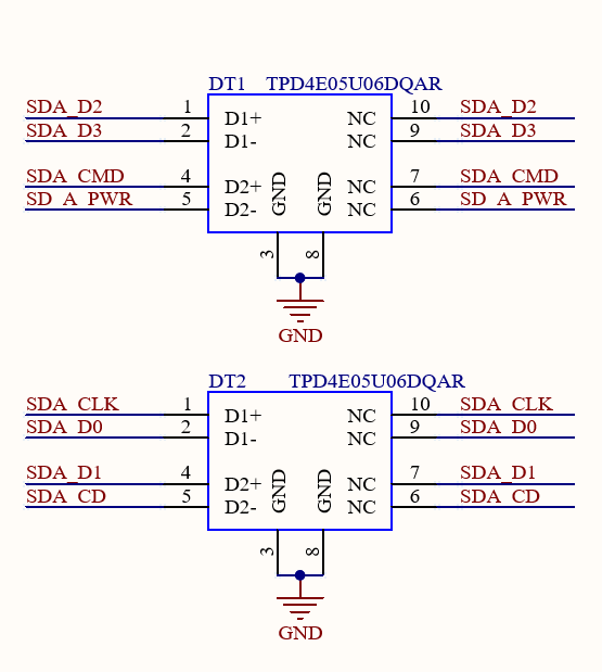
The TF card is a hot-pluggable device. Please add ESD protection for it;
Please make equal length for the SD signal.
3.5.8 USB Download
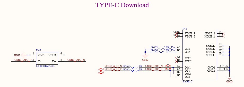
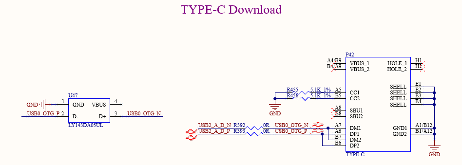
There is a USB Type-C port located at P42 on the back of the development board. It utilizes the P/N differential signals from the USB 3.0_A (pin P19) signal, facilitating connection to a computer for flashing and debugging.
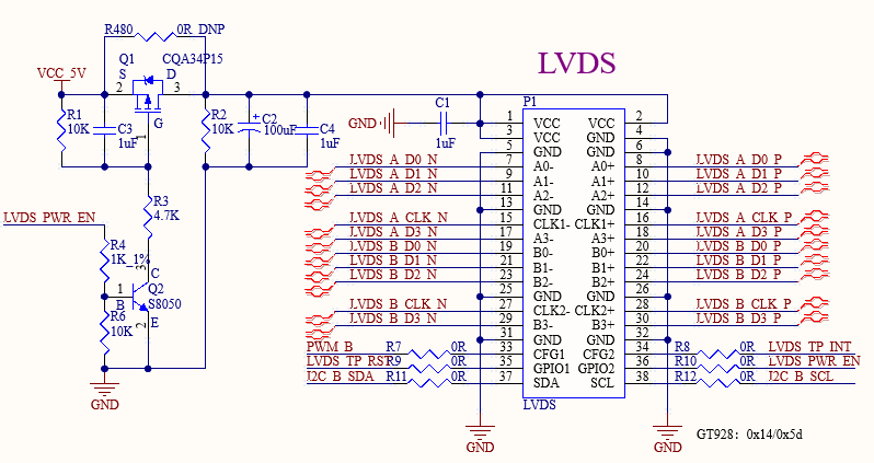
3.5.9 LVDS Display
The pin header P1 on the development board can be connected to the LVDS display via the connector 38P with a pitch of 2.0mm.
It supports 2*4 lane LVDS connection, and I2C port touch screen.
3.5.10 EDP Display
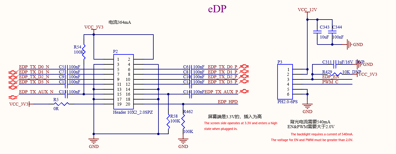
Pins P2 and P3 on the development board can be connected to an eDP display; P2 is with a 2.0mm pitch.
3.5.11 IO
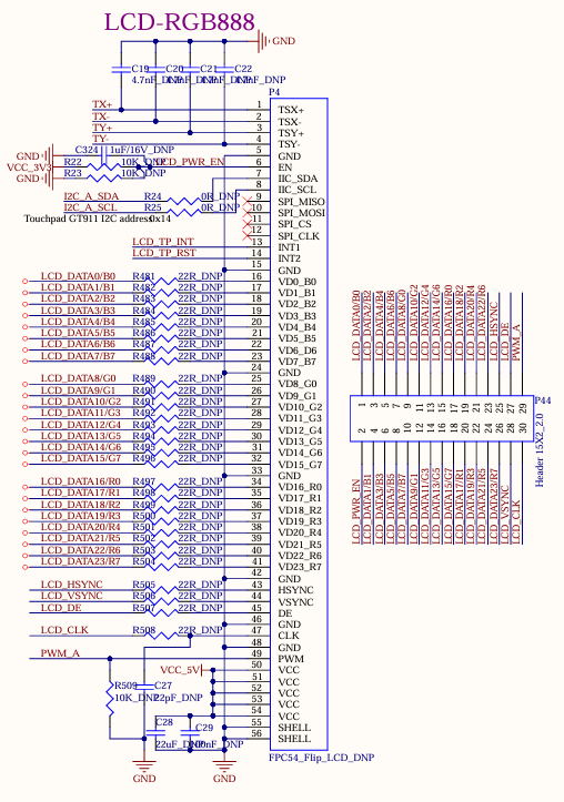
The P44 header on the development board is a 2×15-pin header with a 2.0 pitch, used for I/O testing. The OK527-UP4 carrier board does not support RGB functionality.
3.5.12 HDMI Display
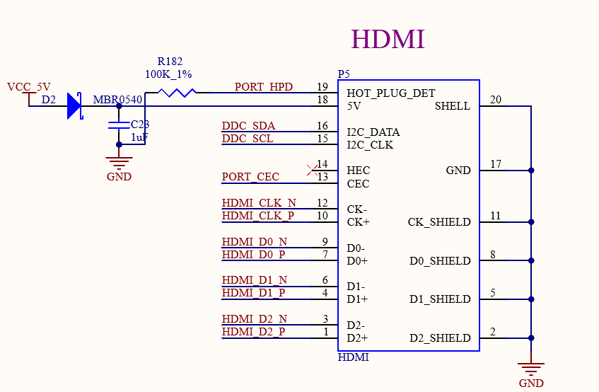
The P5 port on the development board is a standard HDMI port and supports HDMI 2.0.
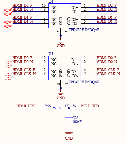
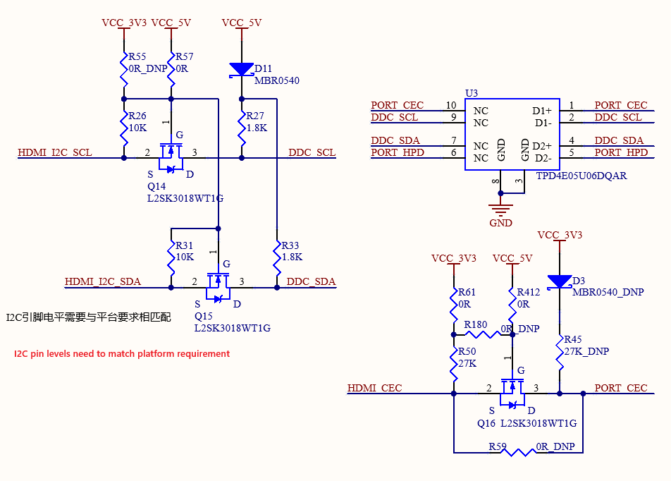
3.5.13 MIPI_DSI
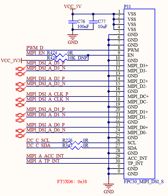
The P11 on the development board is MIPI_DSI port, supporting 4 Lane MIPI_DSI.
3.5.14 MIPI_CSI
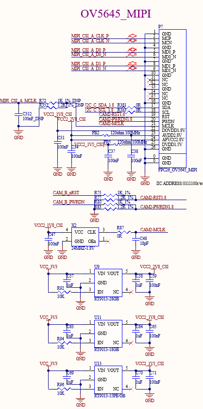
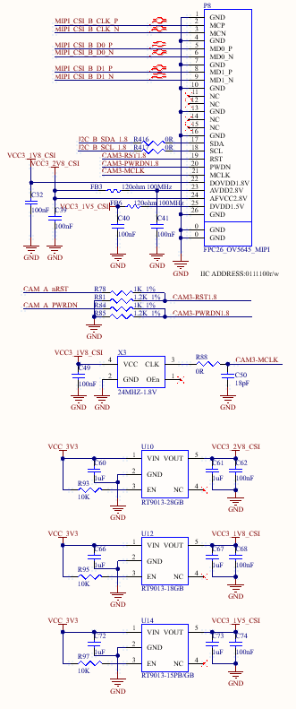
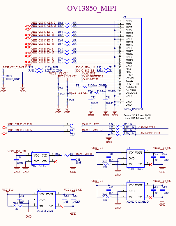
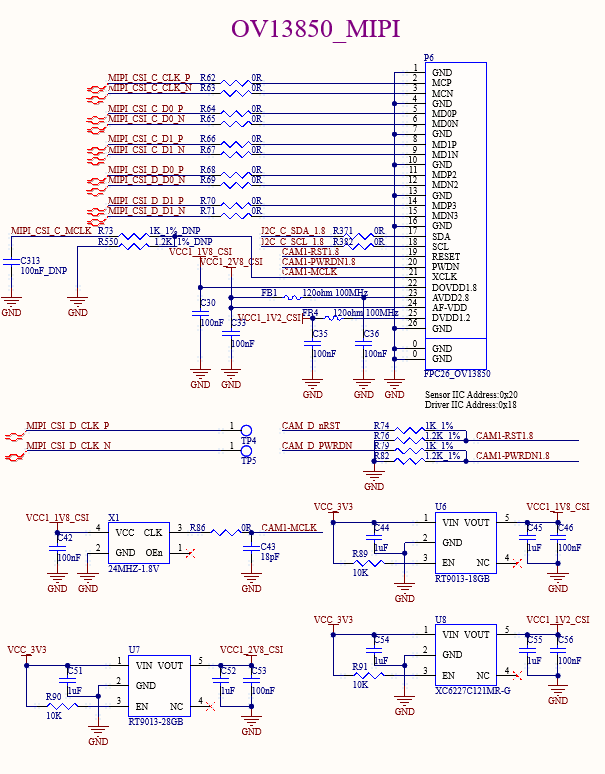
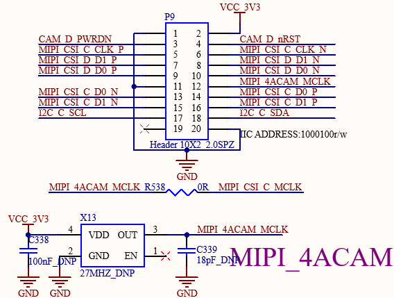
There are there FPC (P6, P7, P8, 0.5mm pitch, with flip cover) on the carrier board for connecting MIPI-CSI camera.
P7 and P8 supports 2lane MIPI-CSI connections.
The P6 port supports 4lane MIPI-CSI connection and multiplexes a signal line with the P9 port. The P9 port is used to connect up to four analogue camera modules. It is not possible to use the P6 and P9 ports for both functions simultaneously.
3.5.15 WIFI&BT
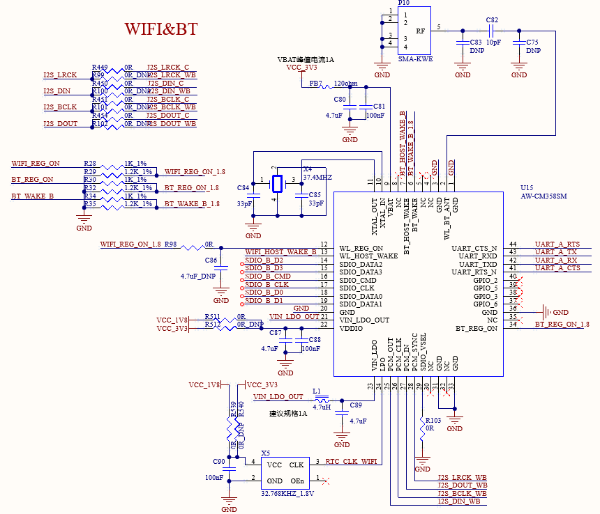
The development board comes with an integrated Wi-Fi & Bluetooth module, model number AW-CM358SM. The Wi-Fi module utilizes an SDIO interface, supports dual-band operation in 2.4GHz and 5GHz, and complies with IEEE 802.11a/b/g/n/ac standards. The Bluetooth module uses UART & PCM interfaces and complies with Bluetooth 5.2 specifications. P10 is an SMA interface for antenna connection. Please use a 2.4GHz&5GHz dual-band antenna.
3.5.16 USB2.0&USB3.0
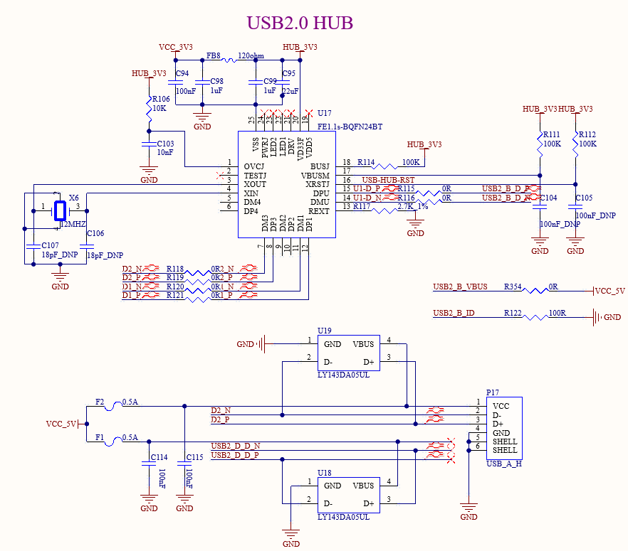
There is an onboard USB 2.0 HUB on the development board, which is expanded to two downstream USB HOST ports, connecting a standard USB 2.0-A interface and a mini-PCIE interface. The mini-PCIE interface can connect the 4G module.
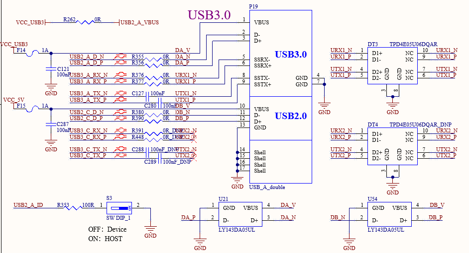
The development board features one USB 3.0 port, which is the SoM’s native USB 3.0 port. A dual-layer USB 3.0 & 2.0 Type-A standard connector is connected to the development board; the Type-A 3.0 port supports OTG, whilst the Type-C 2.0 port (HOST) is routed to the upper layer of the dual-layer USB socket. Route A is controlled by the S3 DIP switch; “OFF” corresponds to “Device” and “ON” to “HOST”.
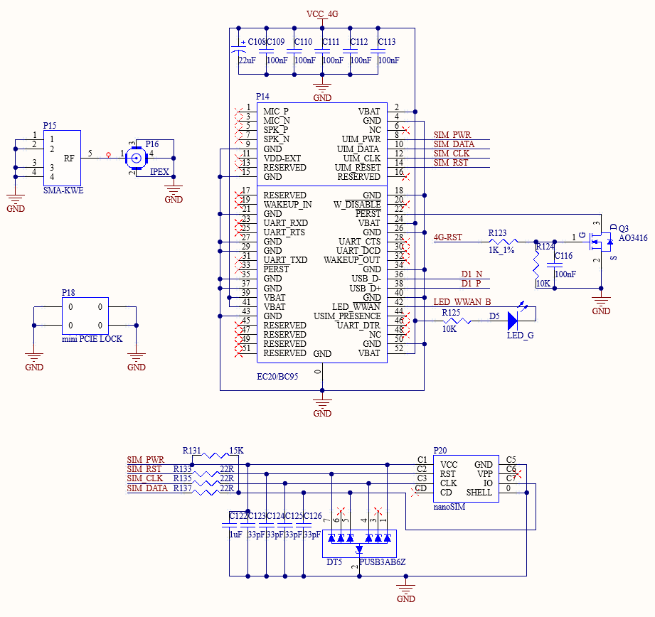
3.5.17 4G
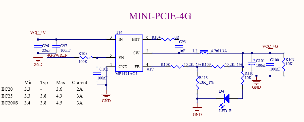
The 4G module can be configured on the development board, and the supported specifications are miniPCIE interface, 3.3 V power supply, and USB2.0 communication.
P20 is a nanoSIM card slot, which is self-ejecting. Pay attention to the insertion direction according to the card identification. It does not support card hot plug.
Before using the 4G function, please power off the board, install the 4G module, the SIM card, and the 4G ipex jumper from the module to the board P15, so that the antenna can be externally connected through the SMA interface of P16.
3.5.18 Ethernet
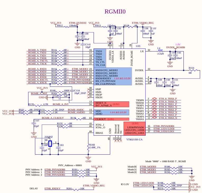
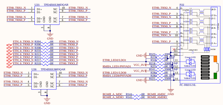
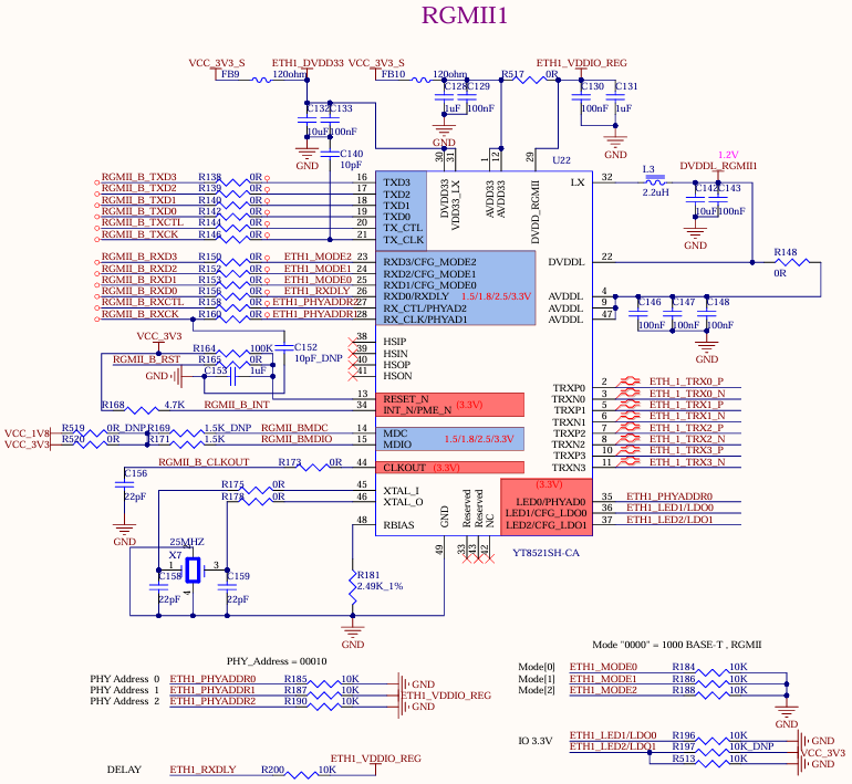
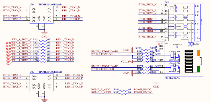
The development board supports two native 1000m network ports, which are realized by using the RGMII of the SoM and the YT8521SH chip, and can be connected to the external network equipment through the standard RJ45 socket with a network transformer.
3.5.19 CAN
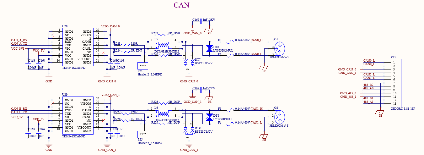
The development board features the native CAN0 and CAN1 pins to provide two standard CAN interfaces. Due to the limitations of the CAN isolation chip, these interfaces support a maximum data rate of 5 Mbps; however, the design incorporates electrical isolation, which meets the protection requirements for most scenarios.
The CAN signal is routed via green terminals with a 3.81 mm pitch; a 120-ohm terminating resistor is installed using a jumper cap.
3.5.20 485
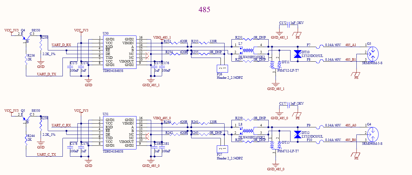
1 x standard 485 is led out from the development board via native UART_C. Due to the UART rate limitation of the CPU, the interface supports a maximum rate of 4Mbps, and the electrical quarantine is designed to meet the protection requirements in most scenarios.
The 485 signal is routed via green terminals with a 3.81 mm pitch; a 120-ohm terminating resistor is installed using a jumper cap.
3.5.21 GPADC
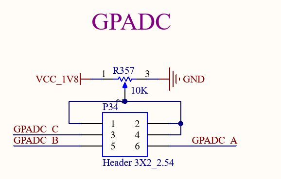
The GPADC is connected via 2.54 mm pitch pins. It can be connected directly using DuPont wires via a potentiometer. The SoM features a total of 3 x GPADC, with a maximum sampling voltage of 1.8 V.
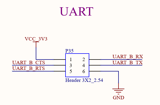
3.5.22 UART
1 x five-wire UART is routed from the development board and powered by a 3.3V signal.
3.5.23 SPI
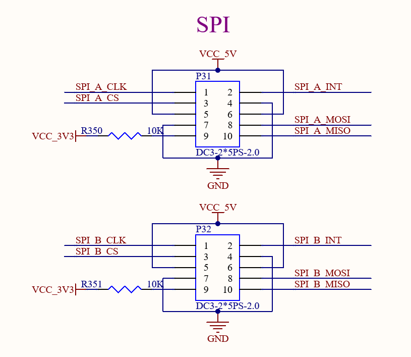
A five-wire SPI interface is led out from the SoM (5V power supply).
3.5.24 IO Expansion
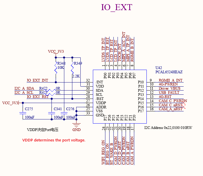
An IO expansion chip is led out from the development board via I2C. 24 additional I/O pins can be expanded for expanding control signals and resetting signals.
3.5.25 Audio
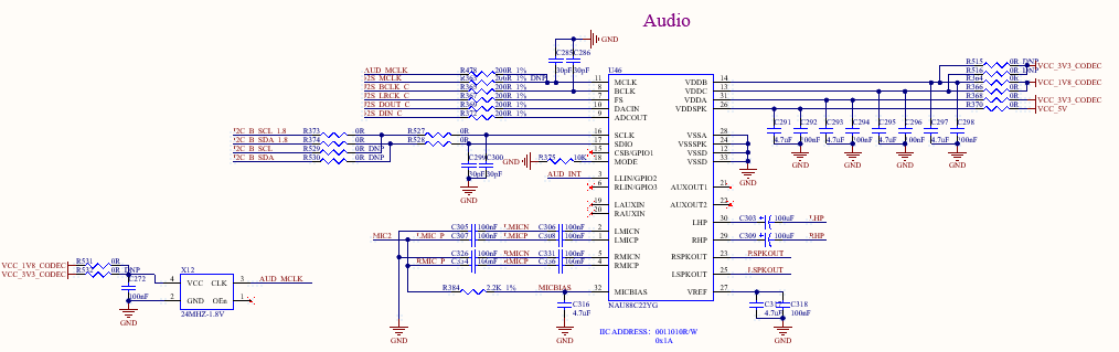
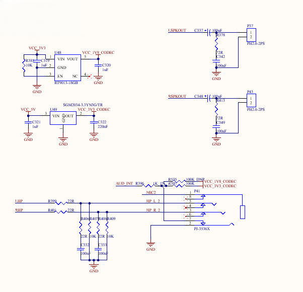
The development board features a standard 3.5mm headphone jack (CTIA international standard), located at pin P40, which supports stereo headphone playback and mono microphone recording;
The P39 and P38 ports are speaker ports, supporting stereo speakers, Class D, with a power output of 1.3W;
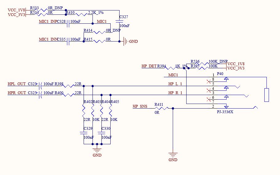
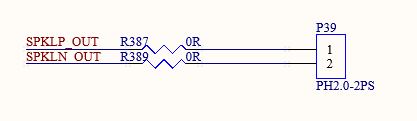
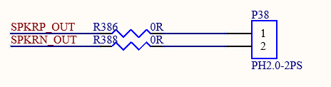
A single I2S signal is routed from the carrier board to the NAU88C22YG CODEC chip, which provides a standard 3.5mm headphone jack and separate left and right channel amplifiers.
4. Package Dimensions Diagram
Package: LCC+LGA
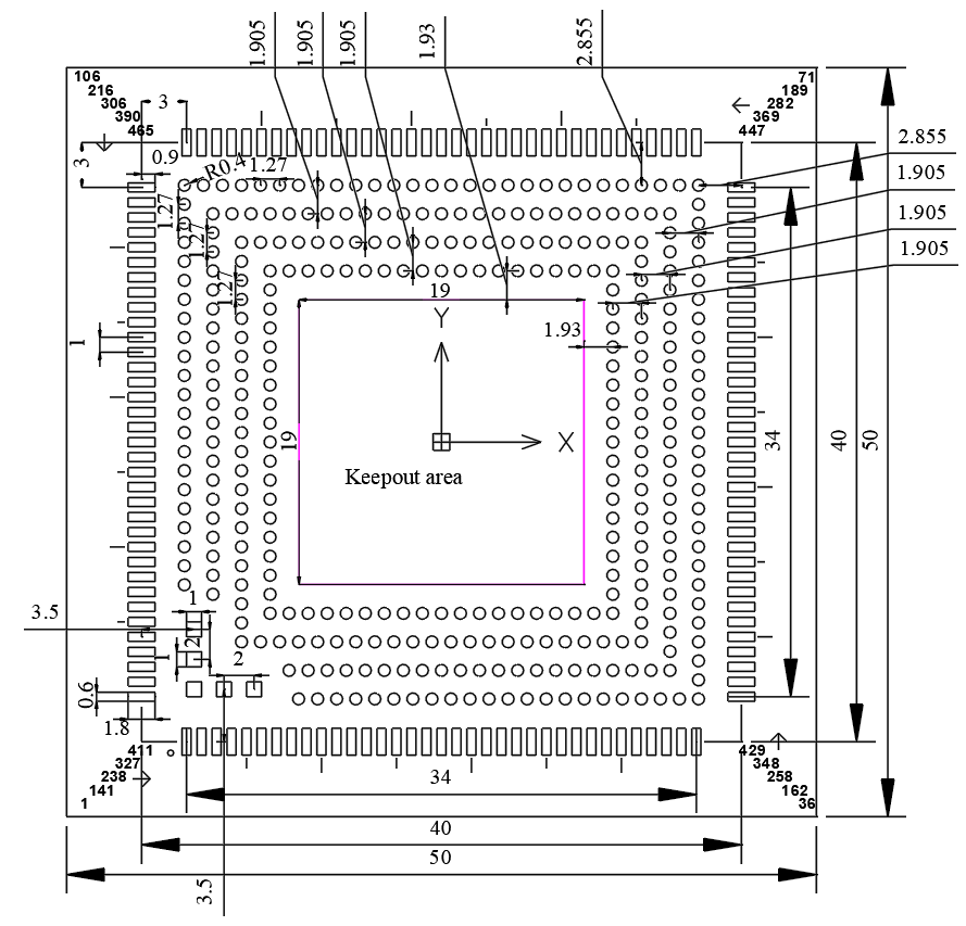
To ensure soldering yield, please refer to the following specifications for stencil design:
Hole Opening Scheme:
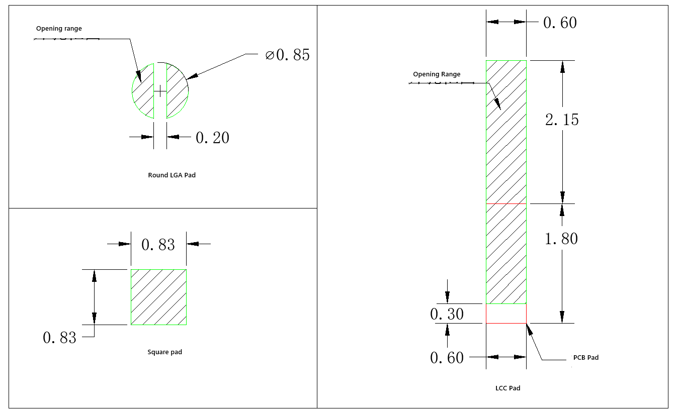
Thickness: Use a 0.1/0.15mm step stencil, with the core board mounting area uniformly designed for a 0.15mm upper step;
LCC Pad Aperture: The opening width should be 0.6mm, and the length should extend outward by 2.15mm along the edge of the pad;
Circular LGA pads: Openings with a diameter of 0.85mm, with a 0.2mm-wide support bridge at the center. Square LGA pads: Openings with dimensions of 0.83mm × 0.83mm.
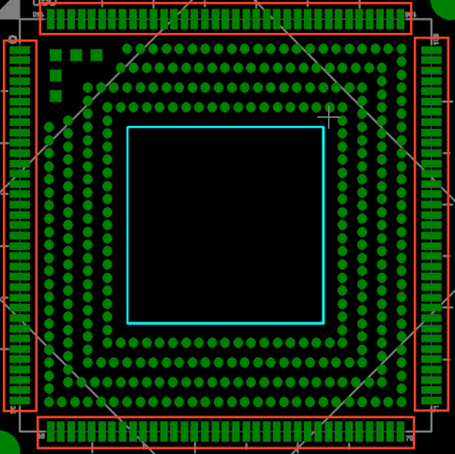
Note:
Since stepped stencils can affect the solder volume on surrounding components, please reduce the aperture size of the stencil openings for these components;
It is recommended to use the official-provided footprint library to avoid design discrepancies.
5. OK527-UP4 Development Board Linux Consumption Table
No. |
Item |
SoM Power (W) |
Development Board Power (including SoM) |
|---|---|---|---|
1 |
No-load startup peak power |
4.485W |
5.196W |
2 |
Sleep mode power consumption |
0.0675W |
0.696W |
3 |
Standby power consumption with no load |
1.375W |
2.244W |
4 |
USB read/write power consumption |
1.555W |
2.964W |
5 |
TF card flashing power consumption |
2.05W |
2.892W |
6 |
4G module PING power consumption |
1.5W |
3.204W |
7 |
WiFi module PING power consumption |
1.48W |
2.28W |
8 |
10-inch LVDS screen power consumption |
1.58W |
6.192W |
9 |
7‑inch MIPI screen video playback power consumption. |
1.46W |
4.452W |
10 |
CPU stress + memory stress + eMMC read/write stress test power consumption. |
5.05W |
5.976W |
Note: The SoM configuration is 2GB memory + +16GB eMMC, the 4G module is Quectel EC20, and the screen is an Forlinx optional product. SoM power supply: 5V; the carrier board is 12V; power consumption is for reference only.
6. Minimum System Diagram
It has SoM, power, debug serial port, system image flashing port.