User’s Hardware Manual_V1.0
Document classification: □ Top secret □ Secret □ Internal information ■ Open
Copyright
The copyright of this manual belongs to Baoding Folinx Embedded Technology Co., Ltd. Without the written permission of our company, no organizations or individuals have the right to copy, distribute, or reproduce any part of this manual in any form, and violators will be held legally responsible.
Forlinx adheres to copyrights of all graphics and texts used in all publications in original or license-free forms.
The drivers and utilities used for the components are subject to the copyrights of the respective manufacturers. The license conditions of the respective manufacturer are to be adhered to. Related license expenses for the operating system and applications should be calculated/declared separately by the related party or its representatives.
Overview
This manual aims to help you quickly get familiar with the product, understand interface functions and configurations. It covers the interface functions and introductions of the development board, product power consumption, and methods for troubleshooting issues during use. Some commands are annotated in the description for user convenience, with a focus on practicality. For information on pin function multiplexing and hardware design guidelines, please refer to Forlinx’s “FET1126B-C& FET1126BJ-C Pin Multiplexing Comparison Table”.
There are four main chapters:
Chapter 1. provides an overall overview of the CPU, briefly introducing its performance and application industries;
Chapter 2. offers a general introduction to the SoM, including descriptions and functions of connector pins;
Chapter 3. introduces the development board in multiple chapters, covering hardware principles and simple design ideas;
Chapter 4. describes the product’s power consumption and other considerations.
Additionally, the manual includes explanations of some symbols and formats.
Format |
Meaning |
|---|---|
Note |
Note or particularly important information must be read carefully. |
📚 |
Relevant explanations regarding the testing section |
️🛤️ |
Related paths. |
Application Scope
This hardware manual applies to Forlinx OK1126B-C&OK1126BJ-C development board (version 1.1 and above) and FET1126B-C, FET1126B-C&FET1126BJ-C SoM (version 1.1 and above).
Revision History
Date |
Version |
SoM Version |
Carrier Board Version |
Revision History |
|---|---|---|---|---|
22/07/2026 |
V1.0 |
V1.1 |
V1.1 |
Initial Version |
1. Rockchip RV1126B Description
1.1 CPU Description
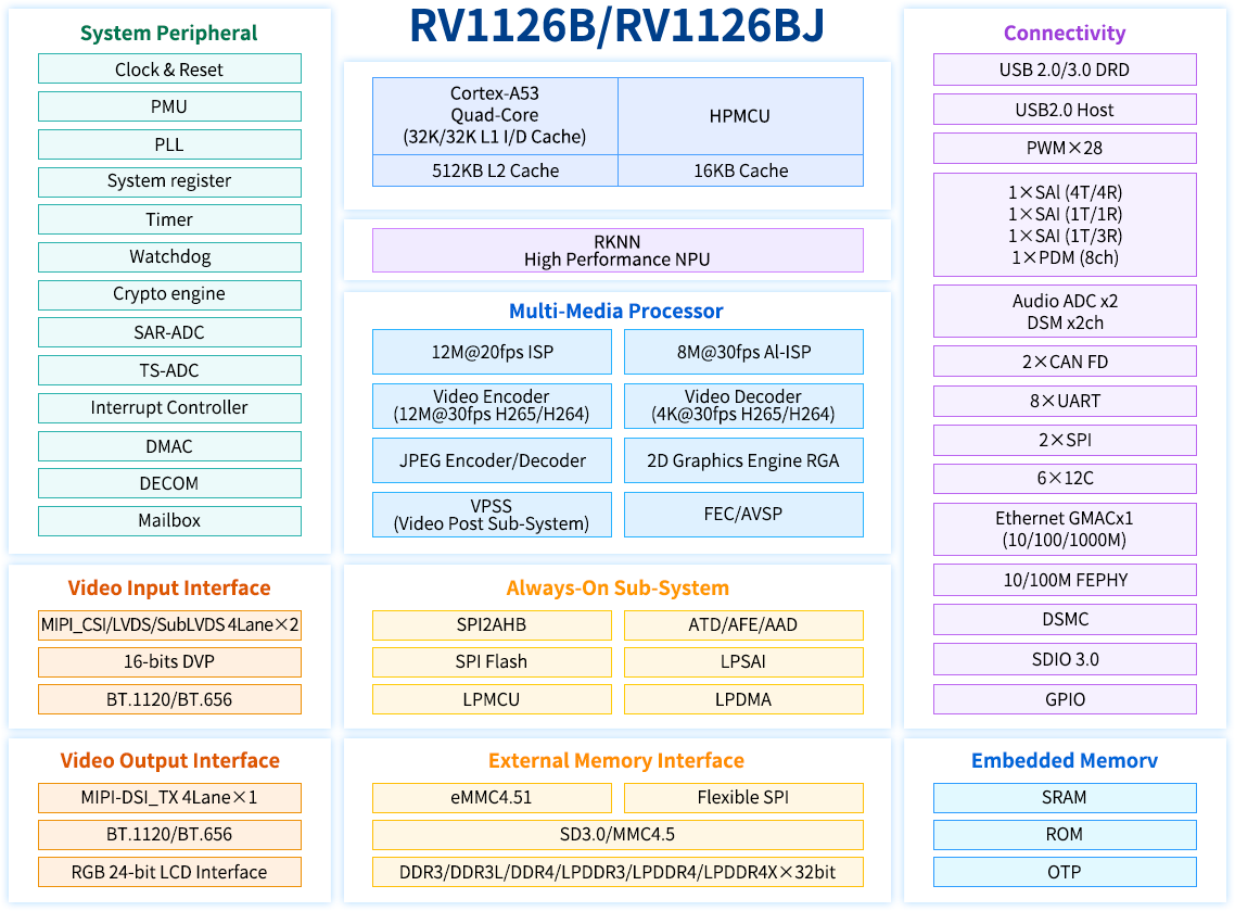
The RV1126B is a high-performance visual processor SoC designed for machine vision applications, particularly AI-related tasks.
It is based on a quad-core ARM Cortex-A53 64-bit architecture, integrated with NEON and FPU. Each core features 32KB of instruction cache and 32KB of data cache, along with a shared 512KB L2 cache. The built-in NPU supports INT8/INT16 mixed-precision computing, delivering up to 3.0 TOPS of computational performance. Additionally, thanks to its strong compatibility, network models based on frameworks such as TensorFlow, MXNet, PyTorch, and Caffe can be easily converted.
The RV1126B introduces a new-generation fully hardware-based ISP (Image Signal Processor) with support for up to 12 megapixels, along with a post-processor. It implements numerous algorithm accelerators, including HDR, 3A, LSC, 3DNR, 2DNR, sharpening, defogging, fisheye correction, gamma correction, feature point detection, and more. Furthermore, it incorporates an AI-ISP supporting up to 8 megapixels, complementing the traditional ISP to deliver superior spatial noise reduction and enhanced image quality. With support for two MIPI CSI (or LVDS/SubLVDS) interfaces and one DVP interface (BT.601/BT.656/BT.1120), you can build systems capable of simultaneously receiving video data from up to four camera sensors.
The built-in video encoder on the RV1126B supports H.265/H.264 video encoding and multi-stream encoding. This feature allows camera video to be encoded at a higher resolution for local storage while simultaneously streaming a lower-resolution version to cloud storage.
The H.264/H.265 video decoder on the RV1126B supports 4Kp30 decoding for both H.264 and H.265. Beyond its high-performance multimedia modules, the RV1126B includes a rich set of audio, memory, and peripheral interfaces, such as I2C, SPI, PWM, and more. These enable users to add additional sensors or peripherals, enhancing system flexibility and scalability.
The RV1126B supports high-performance external DRAM (DDR3/DDR3L/DDR4/LPDDR3/LPDDR4/4X), meeting high-bandwidth memory requirements.
RV1126B Block Diagram
1.2 Introduction to AOV/AOA
AOV (Always On Video) enables 24-hour continuous low-frame-rate recording based on a sleep-wake mechanism. It can switch back to normal frame rate mode when triggered by events such as AI detection, PIR trigger, or Wi‑Fi wake-up. The scenarios are described as follows:
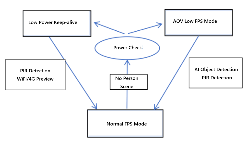
Normal Frame Rate Mode: Activated during remote preview, PIR events, or human detection events. Requires functions such as recording and network connectivity.
AOV Low Frame Rate Mode: Activated during idle periods when battery power is sufficient.
The SoC performs low-frame-rate main-stream recording while maintaining Wi‑Fi/4G connectivity.
Low-Power Keep-Alive Mode: Activated during idle periods when battery power is low.
The SoC powers down while maintaining Wi‑Fi/4G connectivity.
AOA (Always On Audio) utilizes SRAM to cache audio data during sleep, enabling 24-hour continuous audio recording.
2. FET1126B-C SoM Description
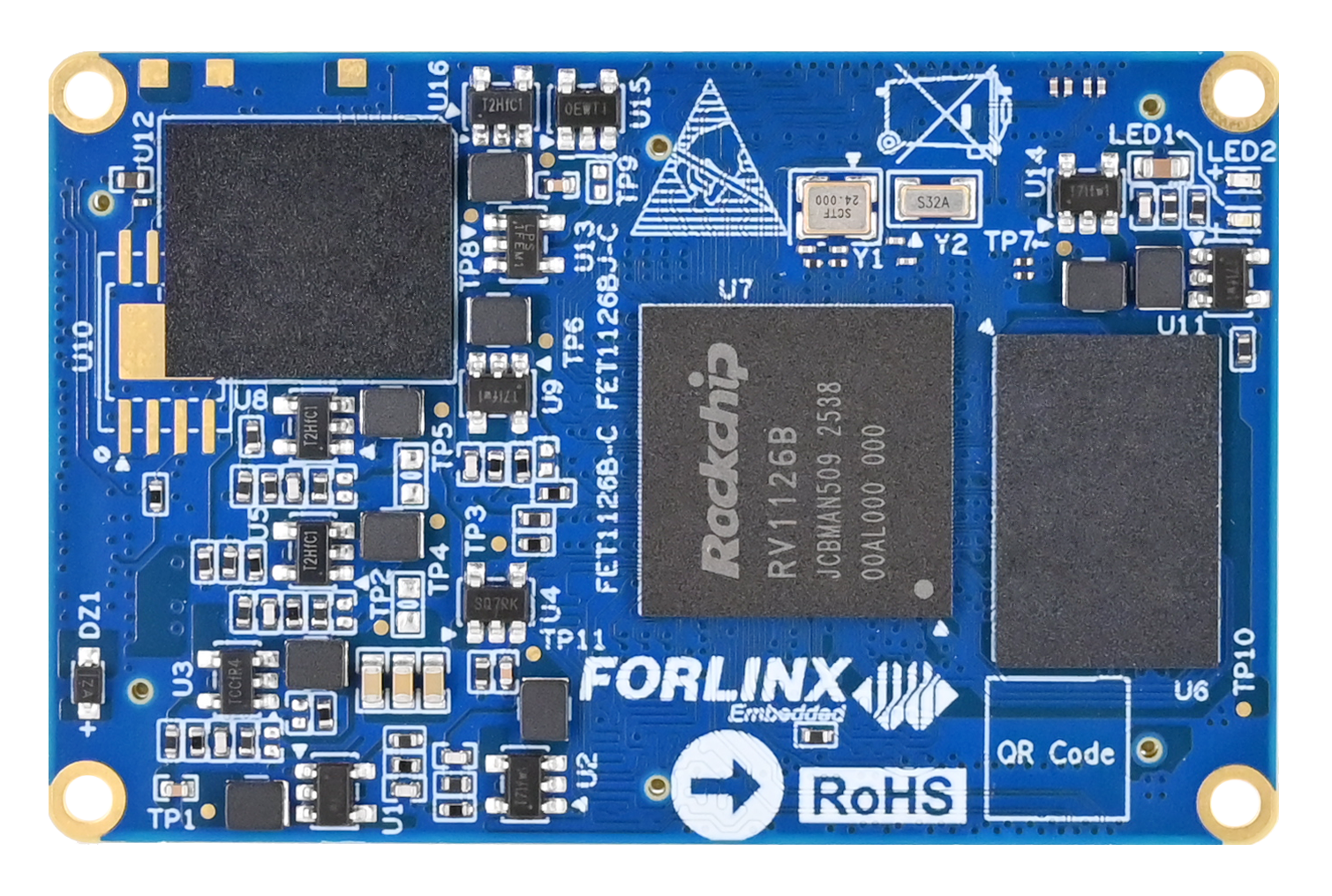
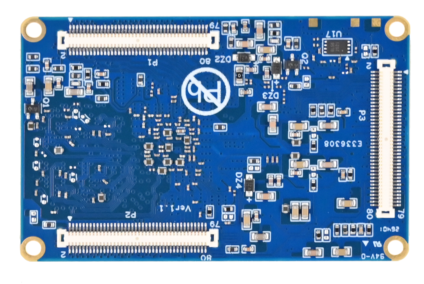
2.1 FET1126B-C Appearance Diagram
Front
Back
2.2 FET1126B-C SoM Dimension Diagram
**FET1126B-C SoM Dimension Diagram: **
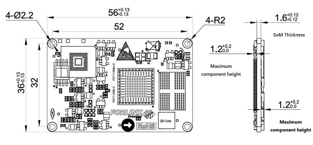
Dimensions: 56mm × 36mm, dimensional tolerance ±0.13mm. For more dimensional details, please refer to the DXF file.
Plate making process: 1.6mm thickness, 10-layer immersion gold PCB.
SoM Connector:
Type: Surface-mounted connector
Pitch: 0.5mm
Pin count: 80P
Gender: Male header, with positioning pillars
Carrier Board Connector:
Type: Surface-mounted connector
Pitch: 0.5mm
Pin count: 80P
Gender: Female socket, with positioning pillars
See Section 04 for the connector dimension drawings.
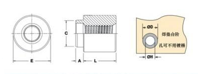
Four 2.2 mm diameter mounting holes are reserved at the four corners of the SoM; when the product is used in a vibration environment, fixing screws can be installed to improve the reliability of product connection. You may refer to the development board design for implementation. On the carrier board, use M2 surface-mount nuts with a length of 2mm. The mounting screws used between the SoM and the carrier board should be M2 screws with a length of 4mm. Please refer to the following illustration for specifications of the surface-mount nuts:

2.3 Performance Parameter
2.3.1 System Frequency
Name |
Specification |
Description |
|||
|---|---|---|---|---|---|
Minimum |
Typical |
Maximum |
Unit |
||
System Frequency |
— |
— |
1.6 |
GHz |
Expand commercial grade |
— |
— |
1.3 |
GHz |
Industrial Level |
|
System RTC |
— |
32.768 |
— |
KHz |
— |
2.3.2 Power Parameter
Parameter |
Pin No. |
Specification |
Description |
|||
|---|---|---|---|---|---|---|
Minimum |
Typical |
Maximum |
Unit |
|||
Main Power Voltage |
VSYS |
4.75 |
5 |
5.25 |
V |
— |
No-load current |
— |
mA |
Please refer to the power consumption table in the appendix |
|||
Overload current |
— |
mA |
Please refer to the power consumption table in the appendix |
2.3.3 Working Environment
Parameter |
Specification |
Description |
||||
|---|---|---|---|---|---|---|
Minimum |
Typical |
Maximum |
Unit |
|||
Operating Temperature |
Working Environment |
-20 |
25 |
+85 |
℃ |
Expand commercial grade |
Storage Environment |
-40 |
25 |
+125 |
℃ |
||
Working Environment |
-40 |
25 |
+85 |
℃ |
Industrial Level |
|
Storage Environment |
-40 |
25 |
+125 |
℃ |
||
Humidity |
Working Environment |
10 |
— |
90 |
%RH |
No Condensation |
Storage Environment |
5 |
— |
95 |
%RH |
2.3.4 SoM Interface Speed
Parameter |
Specification |
Description |
|||
|---|---|---|---|---|---|
Minimum |
Typical |
Maximum |
Unit |
||
Serial Port Communication Speed |
- |
115200 |
4M |
bps |
|
IIC Communication Speed |
- |
100 |
400 |
Kbps |
|
USB Communication Speed |
- |
- |
5 |
Gbps |
2.4 SoM Interfaces
Function |
Quantity |
Parameter |
|---|---|---|
USB |
2 |
1 x USB2.0 Host |
RGB |
≤1 |
Supports RGB 888, up to 1920*1080@60fps. |
MIPI DSI |
≤1 |
4lane, 1.5Gbps/lane. |
MIPI CSI |
≤2 |
Supports 2 x 4lane, 2.5Gbps/lane, can be split into 4 x 2 lanes. |
Ethernet |
≤1 |
Supports either one RGMII interface or a 100M PHY (built into the CPU). |
UART |
≤8 |
The maximum supported baud rate is 4 Mbps; UART1–UART7 support automatic flow control. |
SPI |
≤2 |
Configurable master-slave mode |
SAI |
≤3 |
Can be used for communication with peripherals such as audio ADC, audio DAC, audio codec, and DSP. |
I2C |
≤5 |
Supports 7bits and 10bits address modes up to 1 Mbit/s |
CANFD |
≤2 |
Supports CAN-FD V1.0 and CAN 2.0 A/B; |
PWM |
≤27 |
Supports up to 27 channels of PWM. |
SDIO 3.0 |
≤2 |
1 x TF card slot, supporting high-speed cards; 1 x SDIO interface, 3.3V logic level |
ADC |
≤24 |
24 single-ended inputs, 13bit, 2 MSPS |
DSMC |
≤1 |
One master mode interface is available. |
Audio ADC |
≤2 |
2 x differential MIC inputs, 2 x Audio DSM differential outputs |
GPIO |
≤110 |
110 x GPIO routed out. |
Note: The parameters in the table are the theoretical values of hardware design or CPU.
2.5 FET1126B-C SoM Pin Definitions
2.5.1 FET1126B-C SoM Pin Schematic
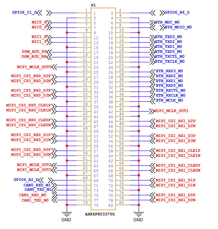
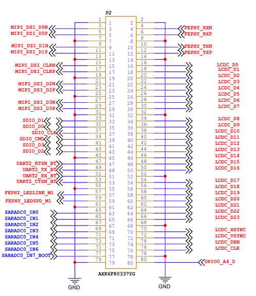
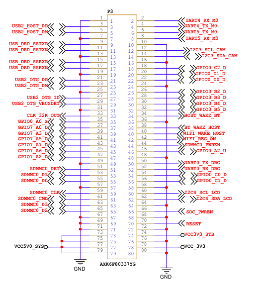
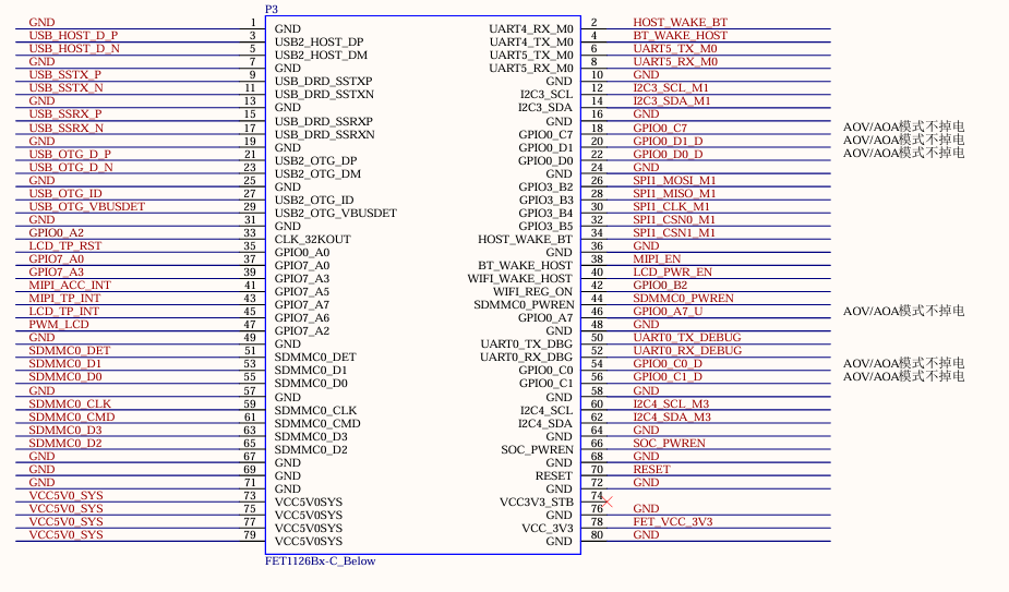
2.5.2 FET1126B-C SoM Pin Function Description
For various functional expansion requirements, please refer to the user document “FET1126B-C& FET1126BJ-C Pin Multiplexing Table”. However, for more detailed information, it is recommended that you consult the relevant documentation, the chip datasheet, and the reference manual.
2.6 SoM Hardware Design Description
Power Pin
Function |
Signal Name |
I/O |
Default Function |
Pin Number |
|---|---|---|---|---|
Power supply |
VCC5V0_SYS |
Power Input |
Power Supply for SoM: |
P3-73;P3-75;P3-77; |
VCC_3V3 |
Power output |
Only used for controlling the power‑on sequence of the carrier board. |
P3-78 |
|
SOC_PWREN |
- |
In sleep (AOV/AOA) scenarios, it serves as an enable control pin for the carrier board power rail that must remain always‑on. |
P3-74 |
|
GND |
Ground |
Power ground and signal ground on the SoM. All GND pins must be connected. |
- |
Note: The VCC3V3_STB pin is prohibited from being used.
System Control Pin
Function |
Signal Name |
I/O |
Default Function |
Pin Number |
|---|---|---|---|---|
CPU reset |
RESET |
I |
SoM power reset, low level effective. |
P3-70 |
BOOT selection |
SARADC0_IN7_BOOT |
I |
When the signal is grounded, the startup card enters the Maskrom download mode. |
P2-77 |
Debug Port |
UART0_TX_DBG UART0_RX_DBG |
I/O |
Debug Port, please keep the port functions. |
P3-50 ; P3-52 |
(Including minimum system block diagram)
The FET1126B-C SoM integrates power, reset monitoring, and storage circuits, requiring only minimal external circuitry. A complete minimum system can be powered and run with a single 5V supply.
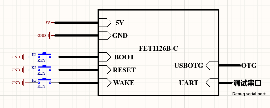
Refer to “Appendix VI. Minimum System Diagram” However, in most cases, it is recommended to connect some external devices—such as a debugging serial port and a port for flashing images—in addition to the minimal system. Otherwise, you can not check whether the system has booted. After completing these steps, you can then add the required functions based on the SoM’s default interface definition provided by Forlinx.
For the design of the SoM’s peripheral circuits, please refer to Section 3.5, “OK1126Bx-C Carrier Board Description”.
3. OK1126Bx-C Embedded Development Description
3.1 OK1126Bx Development Board Interface Diagram
The Forlinx OK1126B-C development board features board-to-board connectors and is compatible with multiple RV1126-series System on Modules (SoMs). Consequently, the PCB silkscreen and this document may use the general designation OK1126Bx-C to refer to this compatible CPU series family. The primary interfaces of the board are illustrated in the figure below.
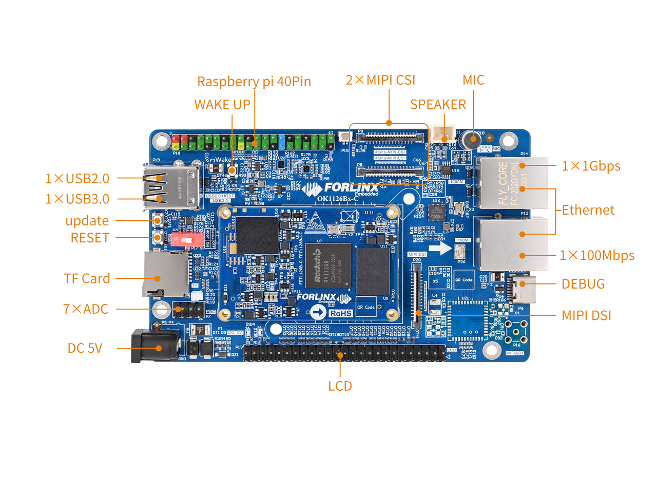 Front
Front
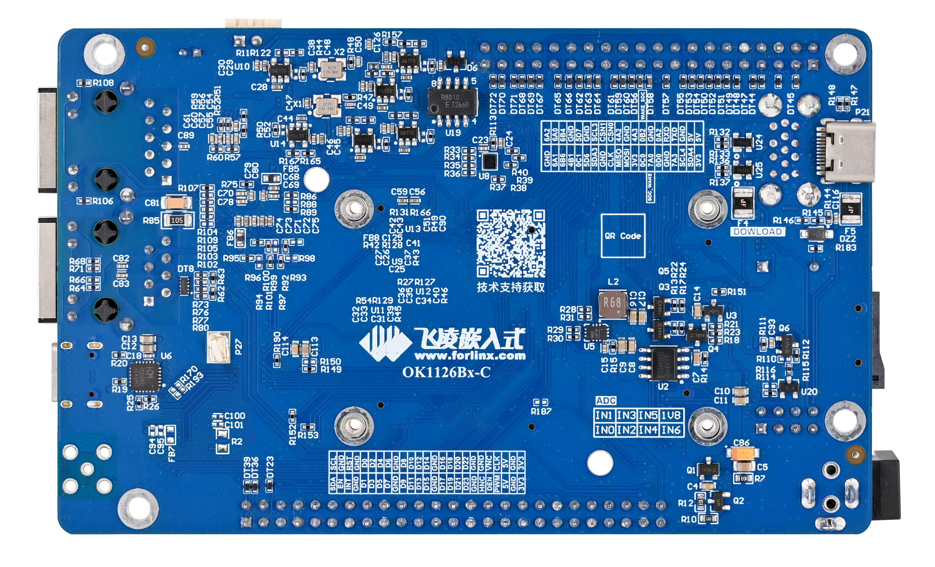
Back
3.2 OK1126Bx Development Board Dimension Diagram
OK1126Bx-C Development Board Dimension Diagram:
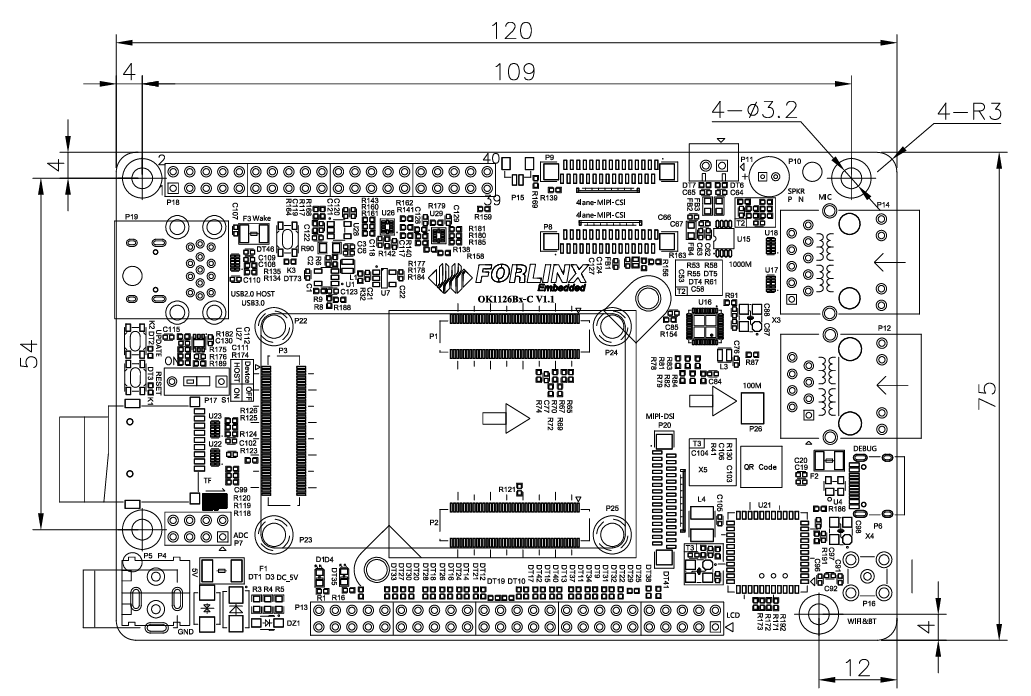
PCB: 120mm×75mm
Mounting hole dimensions: Pitch: 109mm × 54mm, hole diameter: 3.2mm.
Plate making process: 1.6mm thickness, 4-layer PCB.
Power Voltage: DC 5V
3.3 Naming Rules
A B-C+D E F :G-H
Field |
Field Description |
Value |
Description |
|---|---|---|---|
A |
Product Line Identification |
OK |
Forlinx Embedded development board |
- |
Segment Identification |
- |
|
B |
CPU Name |
1126B |
OK1126Bx |
- |
Segment Identification |
- |
|
C |
Connection |
C |
Board to board connector |
+ |
Segment Identification |
+ |
The configuration parameter section follows this identifier. |
D |
Type Label |
M |
Carrier board (Carrier board is marked with M, not filled in by default) |
E |
Operating Temperature |
E |
-20 to 85℃ Commercial-grade |
I |
-40 to 85℃ Industrial-grade |
||
F |
PCB Version |
11 |
V1.1 |
xx |
Vx.x |
||
G |
Internal Identification of the Manufacturer |
:X |
This is the internal identification of the manufacturer and has no impact on the use. |
3.4 Carrier Board Interfaces
Function |
Quantity |
Parameter |
|---|---|---|
TF Card |
1 |
Data rate up to SDR104; |
KEY |
3 |
CPU Reset, Boot Options and Wake-up Button |
UART Debug |
1 |
Integrated into a single Type-C port, enabling connection to a PC for debugging. |
USB2.0 |
2 |
1 x USB_HOST port is connected via a USB socket; |
USB3.0 |
1 |
The USB 3.0 host is connected to the USB 3.0 socket. |
WiFi Bluetooth(1) |
1 |
Single antenna 2.4G&5GHz Wi-Fi Dual-band 1X1 802.11ac +Bluetooth 4.2, |
SPI |
1 |
SPI1 is routed out via the Raspberry Pi’s 40PIN header |
RTC |
1 |
Powered by an external CR2032 button cell; data retention time when power is off |
Ethernet |
1 |
Featuring a standard RJ45 socket, with either a 100 Mbps port or a 1 Gbps port, the RV1126B is equipped with a single GMAC controller. |
UART |
1 |
UART5 is routed out via the Raspberry Pi’s 40PIN header |
I2C |
2 |
I2C3 and I2C4 are connected via the Raspberry Pi’s 40PIN header |
SPEAKER |
1 |
Through the power amplifier chip, it can be connected to an external 4Ω–3.3W speaker. |
MIC |
2 |
One channel is connected to the onboard electret microphone, and the other channel is not externally accessible. |
ADC |
7 |
7 x ADC are routed out via pin headers. |
MIPI-CSI |
2 |
Routed out via an FPC connector, 4 lanes + 4 lanes. |
LCD |
1 |
Routed out via pin headers, supports capacitive touch screens. |
MIPI_DSI |
1 |
4-lane MIPI-DSI, supports capacitive touch screens |
Note:
The parameters in the table are the theoretical values of hardware design or CPU;
WiFi/Bluetooth is currently not supported in this version; the carrier board circuit can be referenced.
3.5 OK1126Bx-C Carrier Board Description
**Note: **
The component UID with “_DNP” mark in the diagram below represents it is not soldered by default;
The schematic diagrams in this manual are only for interface descriptions. Please refer to the source file materials for hardware design.
3.5.1 Carrier Board Power
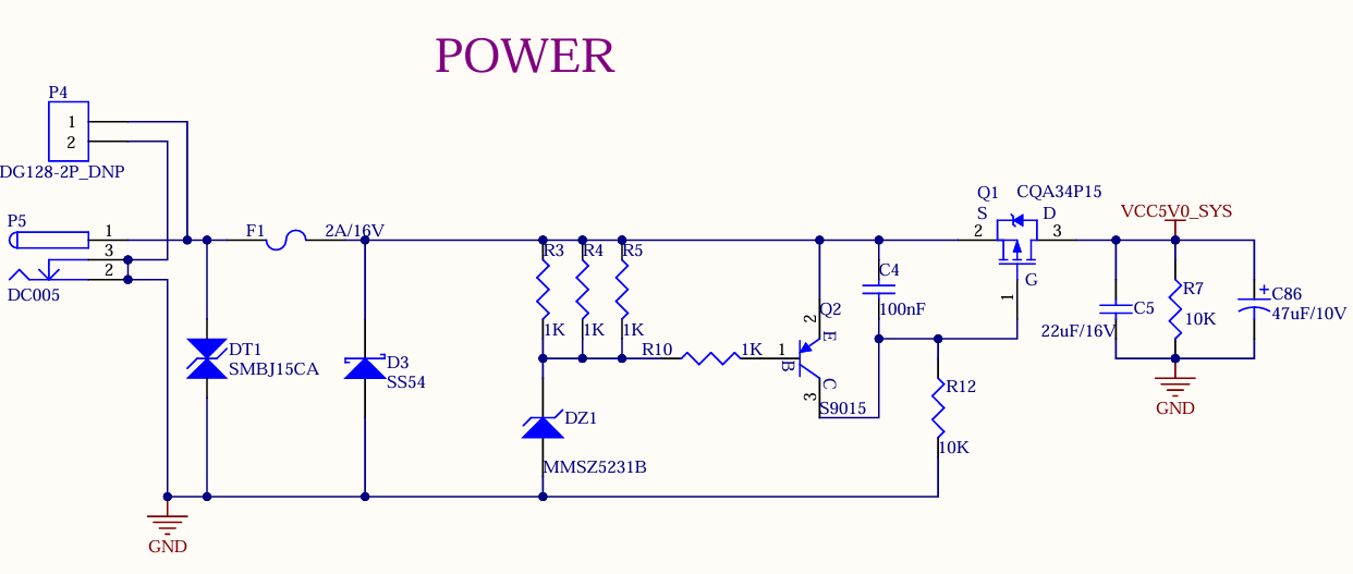
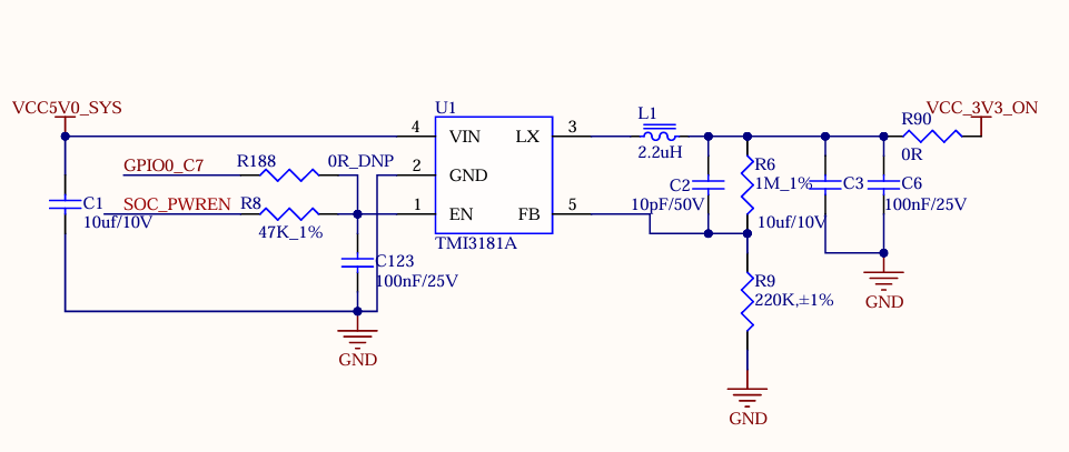
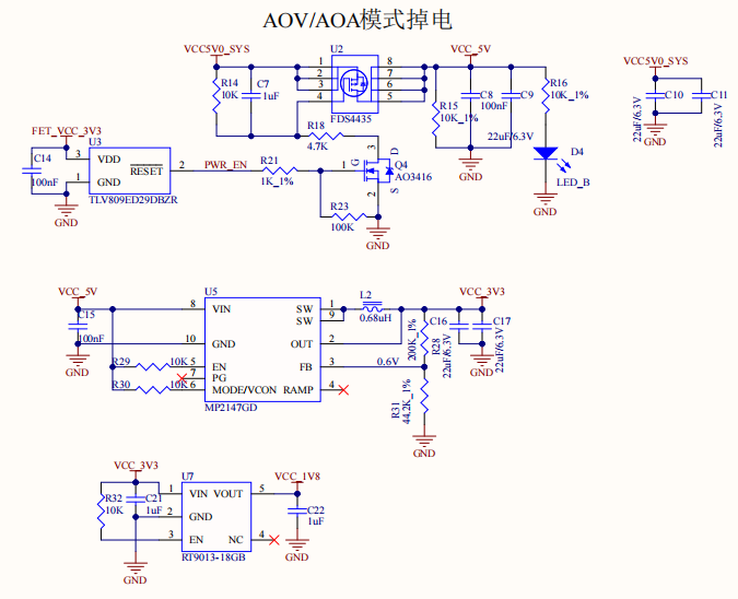
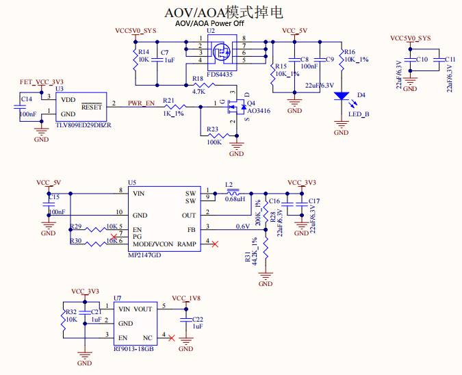
As shown in the figure, the development board is powered by a 5V DC power supply via the DC005 power socket (P5/2-pin) and terminal block P4. A DC 5V power supply passes through a self‑recovery fuse, a reverse‑connection protection diode, and an over‑voltage protection circuit to output VCC5V0_SYS, which powers the SoM. After the SoM is powered on, it outputs FET_VCC_3V3 to enable the carrier‑board U2, thereby supplying VCC_5V, VCC_3V3, and VCC_1V8 to the carrier‑board circuits that are powered off during AOA/AOV modes. Simultaneously, the SoM outputs SOC_PWREN to enable carrier‑board U1, which then outputs VCC_3V3_ON to power the carrier‑board circuits that remain powered during AOA/AOV modes.
FET_VCC_3V3 ensures that the SoM is powered up before the carrier board, preventing latch‑up effects that could damage the CPU. SOC_PWREN serves as the enable control pin for the carrier‑board power rail that must remain continuously powered during sleep (AOV/AOA) scenarios.
Note:
VCC_3V3_ON is a power rail that is not switched off in AOV/AOA sleep scenarios. Its enable pin must be connected to the SOC_PWREN signal from the SoM. If there is no requirement for AOV/AOA sleep operation, this power rail may be ignored.
3.5.2 Reset Buttons
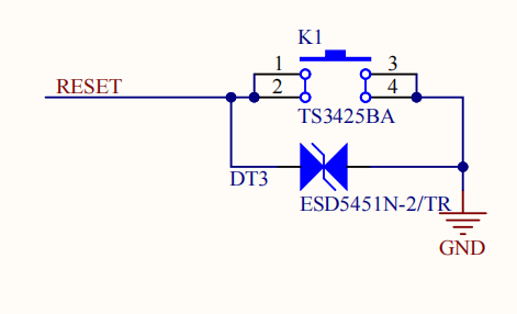
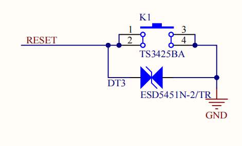
K1 on the development board is the CPU reset button. Pressing it will reset the CPU.
3.5.3 Boot Configuration
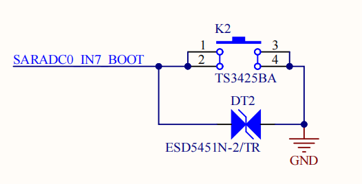
The OK1126Bx‑C determines its boot mode by sampling the voltage on the SARADC0_IN7_BOOT pin. The necessary circuitry for this is already implemented on the core board. The default boot priority order is:
FSPI → eMMC → TF Card → USB.
The FSPI flash memory soldered on the SoM is empty; therefore, the system boots only from eMMC by default. TF Card and USB can be used to burn system images.
USB Burning: Hold down the K4 button while powering on the board to enter Maskrom mode. Then connect USB0 to a computer to burn the system image.
TF Card Burning: First, prepare a TF card with the appropriate burn files. Insert the TF card into the board and power it on; the system will automatically enter the TF‑card burn procedure.
For detailed burning procedures, please refer to the Software User Manual.
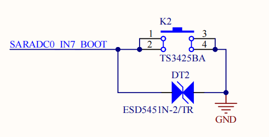
Note: The SARADC0_IN7_BOOT signal must not be used for any other purpose.
3.5.4 SARADC
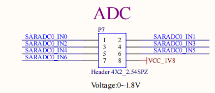
The development board supports 7 ADC channels, which are routed out via a 2.54mm‑pitch pin header P7. Among these, SARADC0_IN0 is pulled up to 1.8V through a 10kΩ resistor on the SoM.
3.5.5 Debugging Serial Port
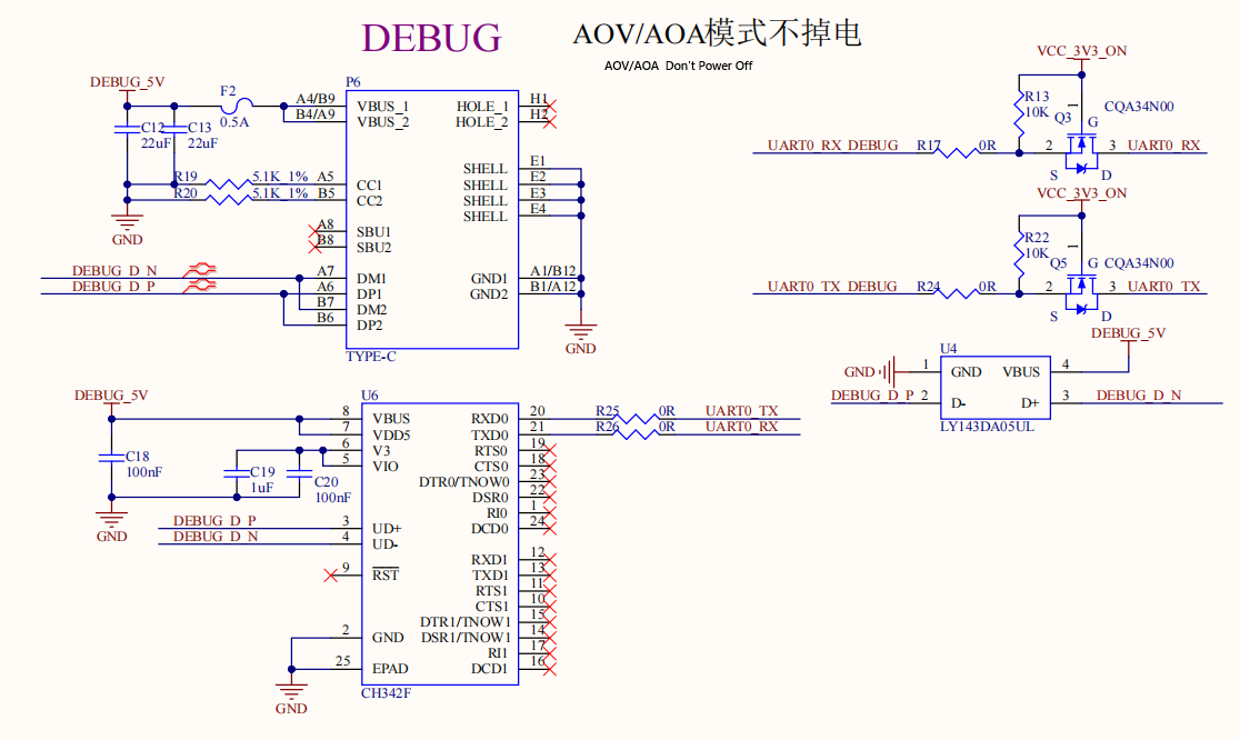
A debug UART is routed out from the development board via a USB Type‑C interface. After installing the CH342 driver on your computer, connecting the P6 port to the PC will enable debugging.
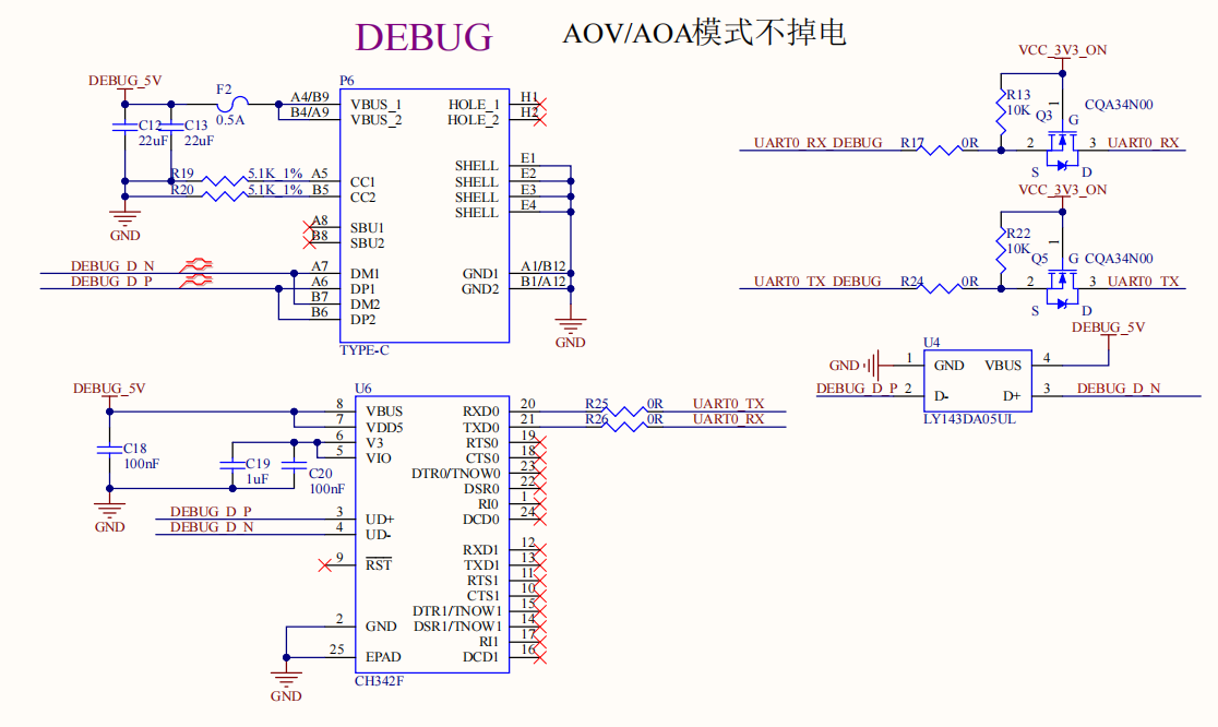
Note: To facilitate debugging later, please ensure that the debugging serial port is led out when designing your own carrier board.
3.5.6 RTC
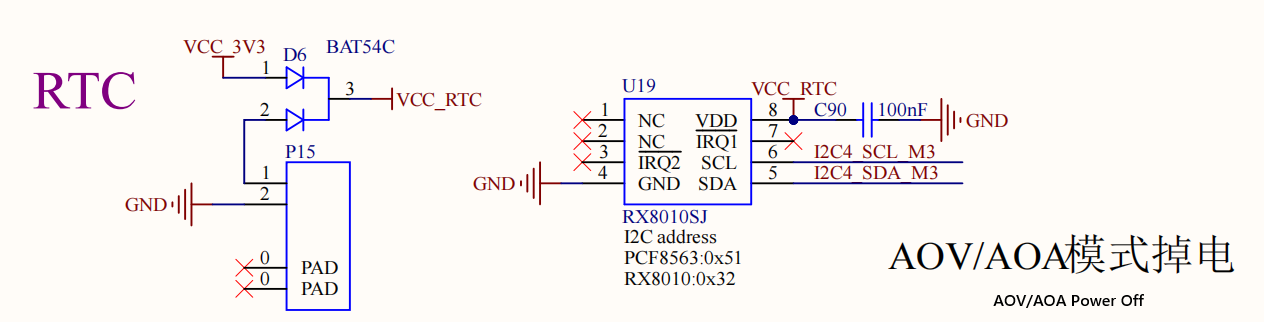
An RTC device is connected externally via I2C4. Power to the RTC is designed to be compatible between VCC_3V3 and a backup coin cell battery (through D6), ensuring that the RTC remains powered after the main board is turned off. The RX8010SJ chip is used in the default design. Button battery: CR2032.
3.5.7 TF Card
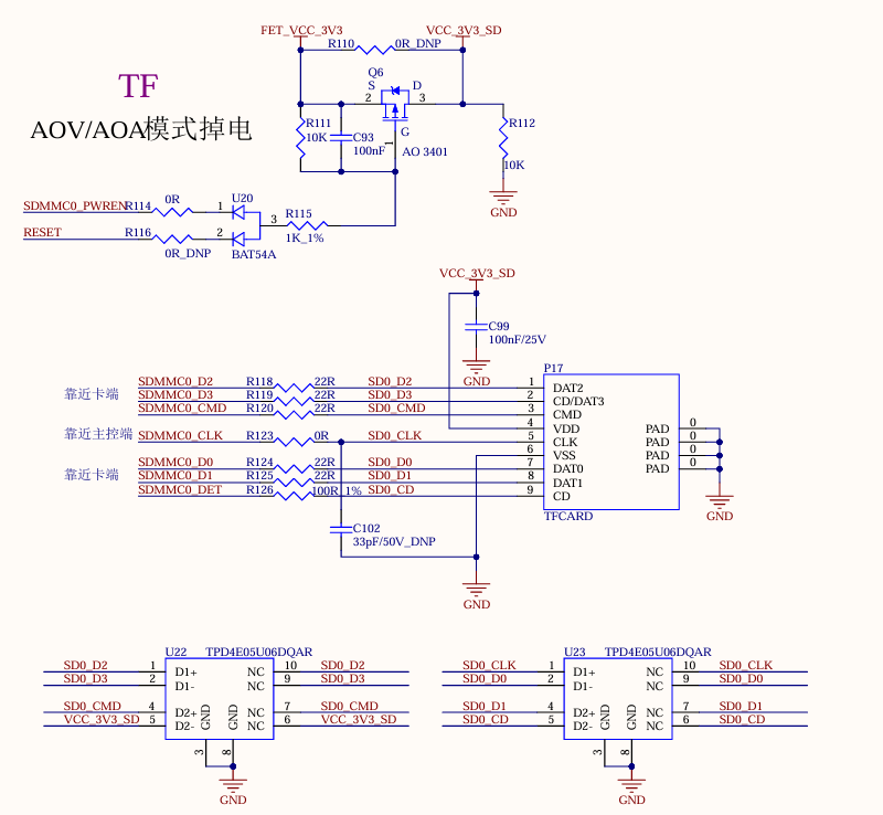
The TF card on the development board is connected to the SDMMC0 channel on the CPU and supports system boot and flashing. The VCC_3V3_SD power supply for the TF card must be regulated; please refer to the carrier board circuit diagram.
Note:
The bus pull-up resistor has already been configured on the SoM. Don’t apply pull-up to the bus on the carrier board;
Since the TF card is a hot‑pluggable device, ESD protection is required;
SD signal lines should be length‑matched;
A 10kΩ discharge resistor should be placed on the TF card power rail to ensure that the power discharges quickly enough after removal. This prevents read errors during rapid card insertion/removal caused by residual charge.
3.5.8 USB2.0 HOST
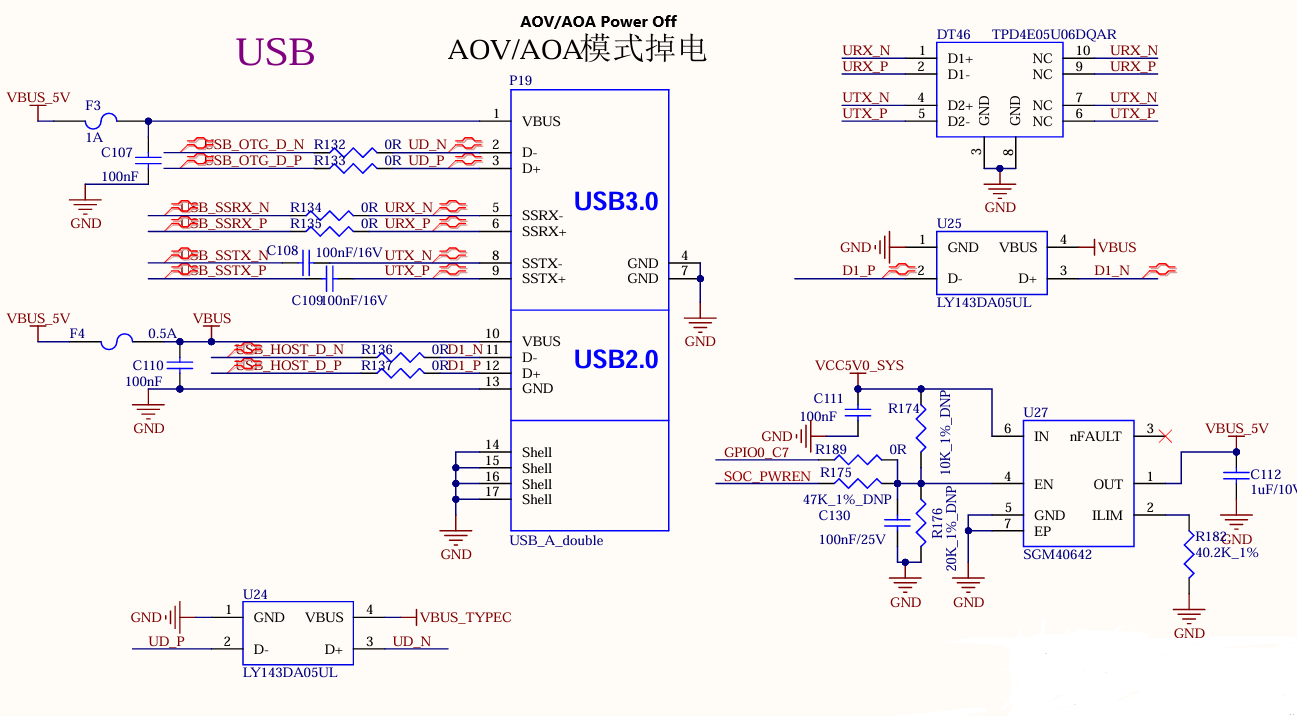
A USB 2.0 port on the carrier board is connected through the USB 2.0 section of the USB-A dual-socket P3, with a current limit of 0.5 A.
Note:
All USB data cables must be designed with a differential impedance of 90Ω;
Please select suitable ESD protection components;
For scenarios where the USB interface must remain powered during AOV/AOA sleep modes (e.g., when connected to an external 4G module), the power supply to this interface must not be cut off during sleep. If control over this power rail is required, it can be managed using a GPIO that remains active during sleep. For details on sleep‑immune GPIOs, refer to the Pin Multiplexing Table.
3.5.9 USB3.0 Interface
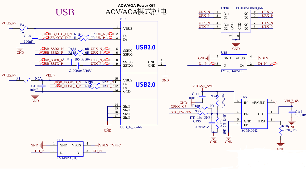
A USB 3.0 port on the carrier board is connected through the USB 3.0 section of the USB-A dual-socket P19, with a current limit of 1 A.
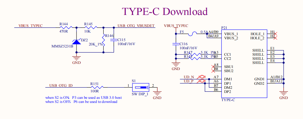
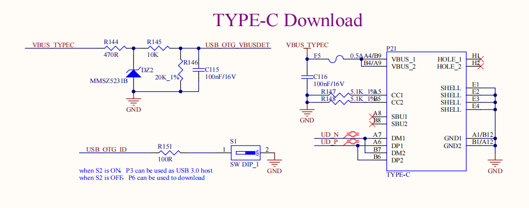
The USB 2.0 signal lines within the USB 3.0 interface are multiplexed with the download interface.
Before the SoM boots, the USB 3.0 OTG defaults to Device mode. When using the USB 2.0 signals to burn an image:
Connect a USB Type‑C cable to socket P21 on the development board.
No ID‑pin configuration is required.
Hold down the K2 button, then power on the board to enter Maskrom mode for system burning.
After the SoM has fully booted, the host/device mode can be toggled via switch S1.
To use USB 3.0 functionality, set S1 to ON and insert the USB device into socket P21.
Note:
Only the SoM native USB 3.0 OTG supports USB system flashing;
All USB data cables must be designed with a differential impedance of 90Ω;
Please select suitable ESD protection components;
USB_OTG_VBUSDET must detect a valid voltage for the USB interface to function normally;
For scenarios where the USB interface must remain powered during AOV/AOA sleep modes (e.g., when connected to an external 4G module), the power supply to this interface must not be cut off during sleep. If control over this power rail is required, it can be managed using a GPIO that remains active during sleep. For details on sleep‑immune GPIOs, refer to the Pin Multiplexing Table.
3.5.10 MIPIDSI
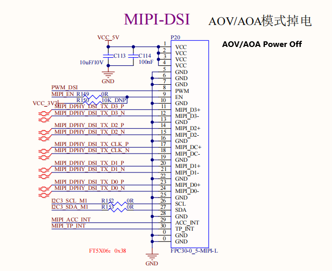
The SoM supports a 4‑lane MIPI DSI interface, with a maximum data rate of 1.5 Gbps per lane and support for resolutions up to 1920 × 1080 @ 60 Hz. The development board features a universal LCD display interface through a 0.5 mm pitch, 30‑pin FPC connector (P20), compatible with Forlinx MIPI capacitive touch screens. Note: The MIPI‑DSI and LCD screen interfaces are mutually exclusive (only one can be used at a time)..
3.5.11 LCD
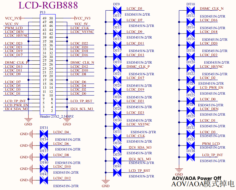
The development board features an LCD interface supporting parallel 24‑bit RGB mode, with a maximum output resolution of 1920 × 1080 @ 60 Hz. The interface is routed out through a 25×2, 2.54 mm pitch pin header (P1). Using an adapter board provided by Forlinx, it can be converted to a 0.5 mm pitch, 54‑pin FPC connector, allowing connection to capacitive touch screens of various specifications produced by Forlinx.
3.5.12 MIPI CSI
The development board supports two 4‑lane MIPI CSI interfaces, both compliant with MIPI V1.2. Each lane supports a maximum data rate of 2.5 Gbps. In practical applications, each 4‑lane port can be split into two independent 2‑lane inputs, enabling simultaneous support for up to four MIPI CSI inputs.
The MIPI CSI functionality is routed out via 30‑pin FPC connectors P8 and P9, which are powered by an independent power supply and are compatible with the OS04A10 camera module.
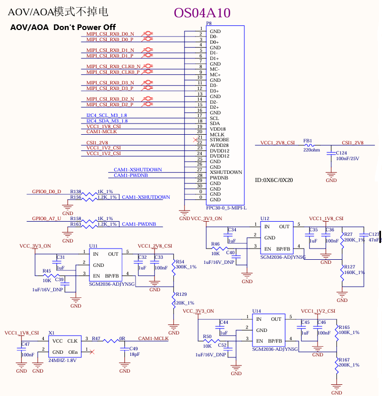
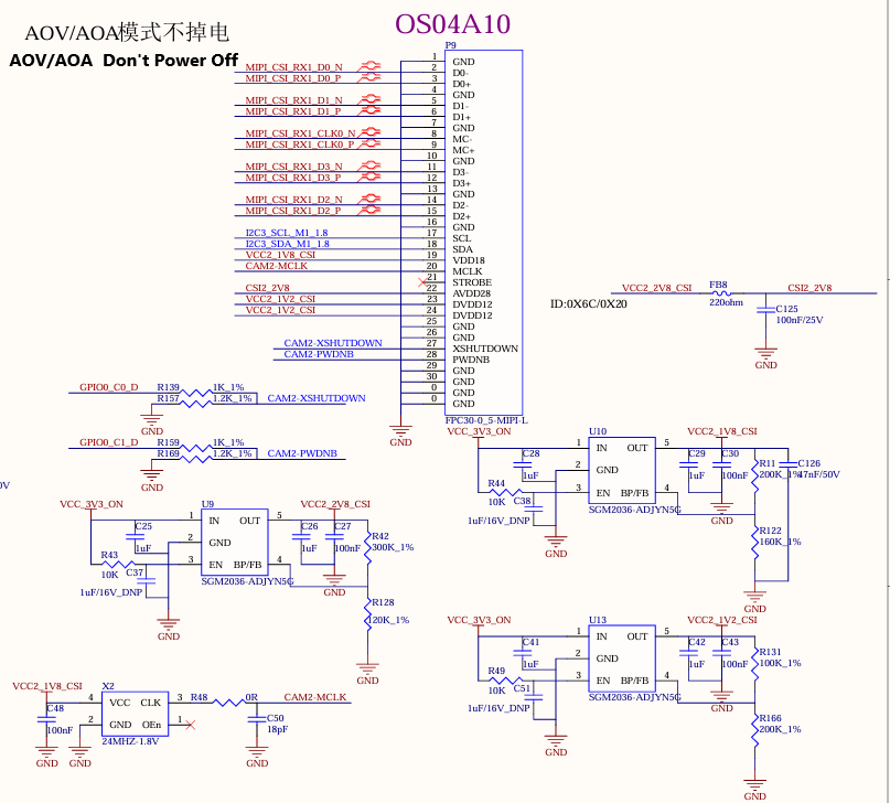
Note: When the MIPI CSI interface is required to operate in AOV/AOA sleep modes, the related power rails for this interface must remain powered during sleep (must not be shut down).
3.5.13 100M Ethernet
The development board supports one 100 Mbps Ethernet port, provided by the CPU’s integrated FEPHY and routed out via an RJ45 connector (model: FC62115BNL), which includes a built‑in isolation transformer.
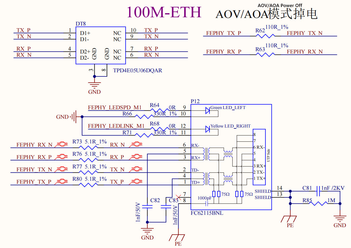
Note:
The RV1126B chip features one GMAC controller, which can provide either an RMII/RGMII interface for connecting an external Ethernet PHY (100M/1000M) or be switched to the internal 100M FEPHY. Only one of these options can be selected at a time; they cannot be used simultaneously. Therefore, on the development board, either the 100M Ethernet port or the 1000M Ethernet port can be used, but not both at the same time;
A 110Ω termination resistor must be placed in parallel between the FEPHY_TXP/N differential pair and between the FEPHY_RXP/N differential pair. This resistor must be placed close to the SoC side and must not be omitted;
5.1Ω series resistors should be placed in line with FEPHY_TXP/N and FEPHY_RXP/N, close to the transformer side, to improve surge immunity;
The 1nF capacitor at the transformer center‑tap must not be changed in value and should be placed close to the transformer.
3.5.14 1000M Ethernet
The development board supports a native 1000M Ethernet port. This is implemented using the SoM’s RGMII interface in conjunction with the MAE0621A-Q3C PHY chip, and is routed through the standard RJ45 connector P14, which integrates a network transformer, for connection to external network devices.
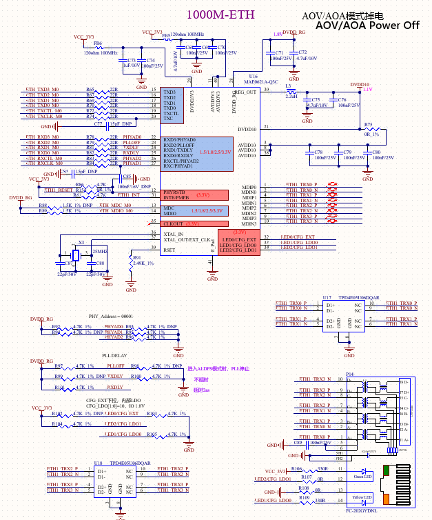
Note:
The RV1126B chip features one GMAC controller, which can provide either an RMII/RGMII interface for connecting an external Ethernet PHY (100M/1000M) or be switched to the internal 100M FEPHY. Only one of these options can be selected at a time; they cannot be used simultaneously. Therefore, on the development board, either the 100M Ethernet port or the 1000M Ethernet port can be used, but not both at the same time;
3.5.15 Audio
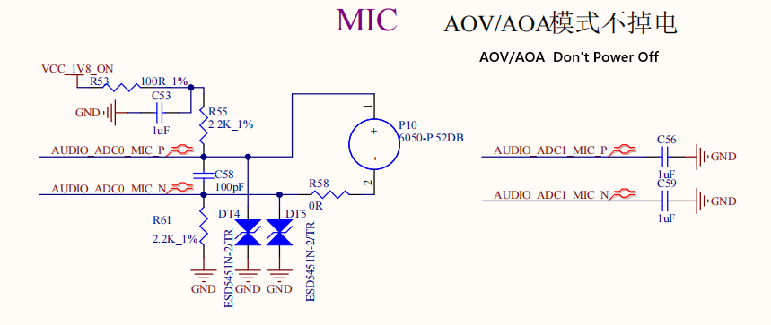
One DSM audio signal is routed out from the development board through an RC low‑pass filter, then amplifies it via the LTK5135M power amplifier, allowing connection to a 4Ω, 3.3W speaker.
A board‑mounted microphone is provided for convenient debugging, supporting monophonic audio recording.
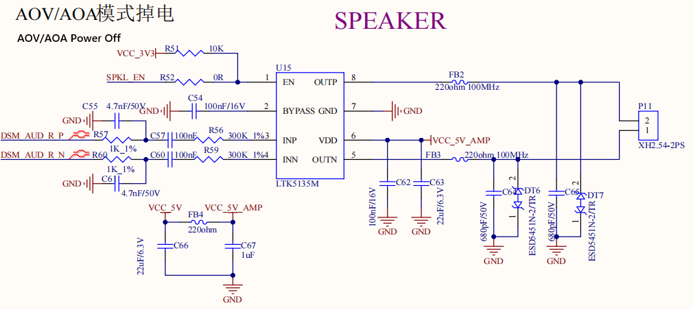
Note:
DSM_AUD_RN/P constitute a differential pair. Both pins must be configured together for the DSM_AUD function; one cannot be assigned to DSM_AUD while the other is used for a different function. The same rule applies to DSM_AUD_LN/P;
When the MIC interface is required to operate in AOV/AOA sleep modes, its associated power supply must remain on during sleep (must not be shut down).
3.5.16 WiFi & Bluetooth (Not supported in this version)
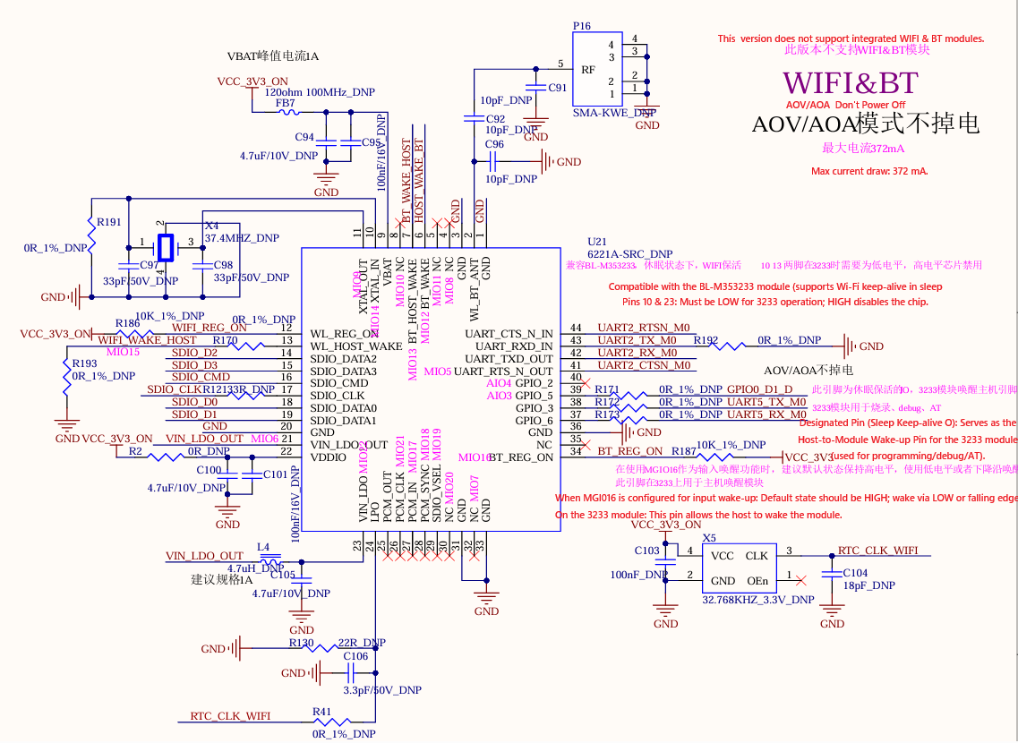
The development board features an onboard WiFi & Bluetooth combo module, model Fn‑Link 6221A‑SRC. The Wi-Fi module uses an SDIO interface, supports dual bands (2.4GHz and 5GHz), and complies with IEEE 802.11a/b/g/n/ac; the Bluetooth module uses a UART interface and complies with Bluetooth 4.2 Module.
P16 is an SMA interface for antenna connection. Please use a 2.4GHz&5GHz dual-band antenna.
Note:
The functionality of this module is not supported in this version; the related circuitry and component selection are for reference only.
3.5.17 Raspberry Pi 40PIN
A 40-pin header (P16) is reserved on the carrier board that is compatible with the Raspberry Pi 40-pin definition. Each pin is equipped with ESD protection.
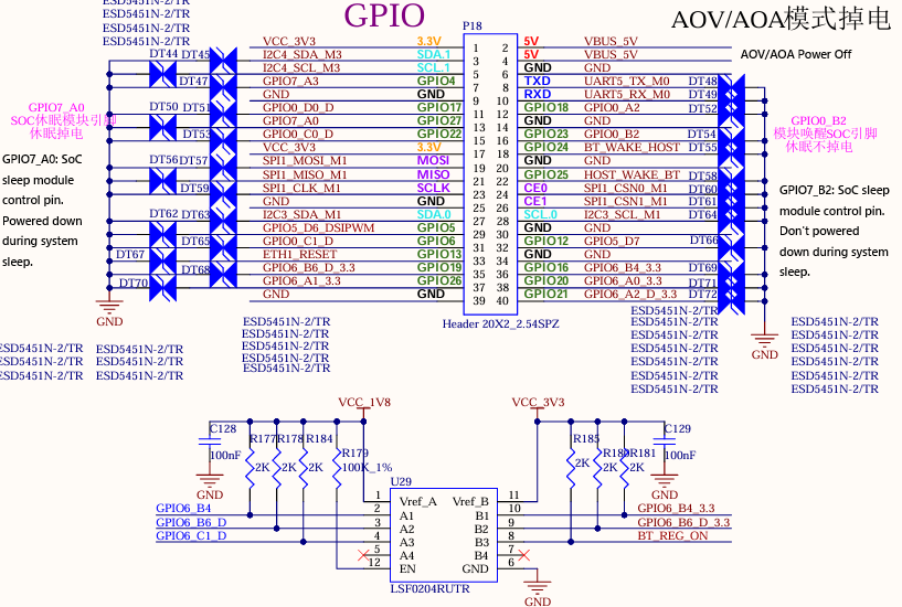
Note: This interface includes GPIOs that can operate normally during sleep (AOV/AOA) scenarios, such as GPIO0_B2.
3.5.18 WAKE UP Button
A physical WAKE UP button is reserved on the carrier board to enable physical wake-up from sleep mode.
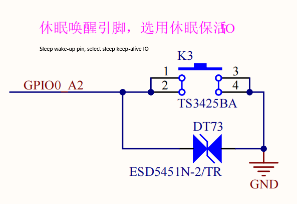
Note: This pin must use a GPIO with sleep-preservation. For details on sleep‑immune GPIOs, refer to the Pin Multiplexing Table.
4. Connector Specification Diagram
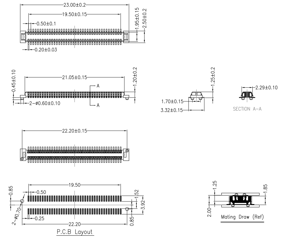
SoM connector: surface-mount, 0.5mm pitch, 80P, male, 1.23mm height, with locating posts.
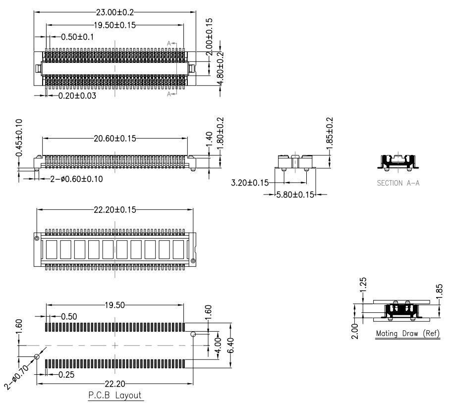
Carrier board connector: surface-mount, 0.5mm pitch, 80P, female socket, 1.85mm height, with locating posts.
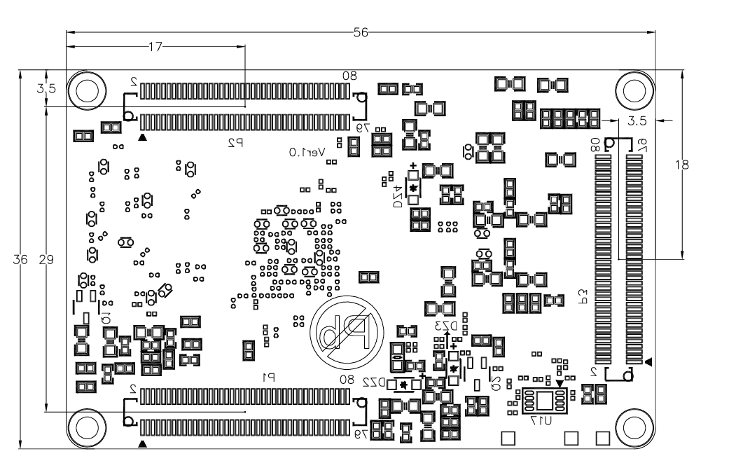
SoM connector location map:
5. OK1126Bx-C Development Board Power Consumption Table
Table 1 OK1126B-C Linux Power Consumption
No. |
Test Item |
SoM Power (W) |
Development Board Power (including SoM) |
|---|---|---|---|
1 |
No-load startup peak power |
1.86W |
2.32W |
2 |
No-load standby |
0.44W |
1.18W |
3 |
Sleep mode |
0.36W |
0.58W |
4 |
USB Read and Write |
0.54W |
2.20W |
5 |
TF card read and write |
0.75W |
1.52W |
6 |
Network Port PING |
0.65W |
1.78W |
7 |
Camera with a load |
0.72W |
2W |
8 |
Load 7-inch MIPI screen + play video |
0.95W |
5.65W |
9 |
On-load camera + on-load 7-inch MIPI screen + video playback |
1.15W |
6.43W |
10 |
CPU with full load |
1.54W |
2.3W |
11 |
Memory is full |
1.06W |
1.82W |
12 |
EMMC Read and Write |
1.24W |
1.98W |
13 |
CPU stress + memory stress + eMMC read/write stress test power consumption. |
1.84W |
2.79W |
14 |
AOV mode + camera + sleep mode |
0.007W |
0.065W |
15 |
AOV mode + camera + face recognition |
1.01W |
1.65W |
Note:
The SoM configuration is 2GB memory+16GB eMMC, and the screen is an Forlinx optional product. SoM power supply: 5V; and the carrier board is 5V;
Power consumption is for reference only.
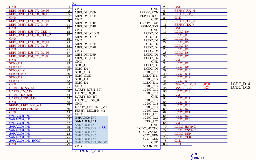
6. Minimum System Diagram
It has SoM, power, debug serial port, system image flashing port.
During SoM design, power-on startup is supported as long as the 5V main power of the SoM is available. However, to ensure the ability to program the SoM and view debugging/print information, it is recommended to retain the following circuits:
- Boot selection circuit
- USB programming circuit or TF card programming circuit
- DEBUG circuit
- Reset button
Note: The reset button must not include a pull‑up resistor in its design.


7. User Hardware Design Guide
I2C Requirements
Multiple slave devices can be connected to a single I2C bus; ensure there are no address conflicts.
Pull-up resistors are required on the I2C bus, but avoid using multiple resistors for pull-up (i.e., use a single pair of pull-up resistors for the entire bus).
Ensure level matching between the I2C signals from the SoM and those from the slave devices.
I2C/UART/CAN/SPI Interface Group Selection
On the SoM, pins for interfaces such as I2C, UART, CAN, and SPI are multiplexed across different power domains. Different multiplexing positions are distinguished by suffixes _M0, _M1, etc. _M0 and _M1 cannot be used simultaneously. When allocating pins, only one group can be selected; it is not allowed to mix signals from M0 and M1 groups.
If a function name includes a suffix such as M0, M1, or M2, it indicates that the same function is multiplexed across different IOs, and only one of them can be selected at a time. For example, when selecting the UART2 function, the combination UART2_TX_M0 and UART2_RX_M0 must be used; combinations like UART2_TX_M0 and UART2_RX_M1 are not supported.
1000M/100M Ethernet Port Selection
The RV1126B chip features one GMAC controller**,** which can provide either an RMII/RGMII interface for connecting an external Ethernet PHY (100M/1000M) or be switched to the internal 100M FEPHY. Only one of these options can be selected at a time; they cannot be used simultaneously.
WiFi & BT Module Design
The WiFi & BT module is supported in AOV mode. Pay attention to the module selection: choose a WiFi & BT module with sleep functionality to prevent current backflow through the connected I/O pins during AOV mode. Alternatively, consider using an independent power supply for the WiFi & BT module, controlled via a keep-alive I/O signal to enable power during sleep.
Hardware Design Requirements for Sleep (AOV/AOA) Scenarios
For interfaces involved in sleep (AOV/AOA) scenarios, their power supply must remain always-on.
To ensure overall power sequencing, the enable control for this always-on power supply should use either the SOC_PWREN signal or a GPIO signal that remains powered during sleep.
For scenarios where a keep-alive peripheral needs to wake up the CPU, the connecting signals must be GPIOs that remain powered during sleep.
Additionally, if a keep-alive peripheral is connected to regular GPIOs (which lose power during sleep), the peripheral’s IOs should be switched to high-impedance state. Otherwise, leakage current may flow back into the SoM and cause malfunctions.